Introduction to PCB Through-Holes
Printed Circuit Boards (PCBs) are the backbone of modern electronics, providing a platform for components to be mounted and interconnected. One of the essential features of PCBs is through-holes, which play a crucial role in component placement and electrical connectivity. In this article, we will explore the concept of PCB through-holes, their types, manufacturing process, and their importance in PCB design and assembly.
What are PCB Through-Holes?
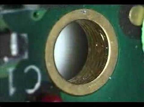
PCB through-holes are small, drilled holes that pass completely through the PCB, allowing components to be inserted and soldered onto the board. These holes provide electrical and mechanical connections between different layers of the PCB, enabling the creation of complex circuits and the mounting of various components such as resistors, capacitors, and integrated circuits (ICs).
Types of PCB Through-Holes
There are two main types of PCB through-holes:
-
Plated Through-Holes (PTHs): PTHs are the most common type of through-holes used in PCBs. They are drilled holes that are electroplated with a conductive material, typically copper, to create an electrical connection between the layers of the PCB. PTHs are used for both component mounting and electrical interconnectivity.
-
Non-Plated Through-Holes (NPTHs): NPTHs are drilled holes that are not electroplated with a conductive material. They are primarily used for mechanical purposes, such as mounting hardware or providing ventilation. NPTHs do not provide electrical connectivity between the layers of the PCB.
Manufacturing Process of PCB Through-Holes
The manufacturing process of PCB through-holes involves several steps:
Drilling
The first step in creating through-holes is drilling the holes into the PCB Substrate. This is typically done using high-speed, computer-controlled drilling machines that can accurately drill holes with diameters ranging from 0.1mm to 6.35mm. The drilling process is critical, as the hole size and position must be precise to ensure proper component placement and electrical connectivity.
Deburring and Cleaning
After drilling, the holes are deburred to remove any rough edges or debris that may interfere with the Plating process. The PCB is then cleaned to remove any contaminants or residue that may affect the plating quality.
Electroplating (for PTHs)
For PTHs, the next step is electroplating the holes with a conductive material, typically copper. The PCB is immersed in an electroplating solution, and an electrical current is applied, causing the copper to adhere to the walls of the holes. This process creates a conductive pathway between the layers of the PCB.
Finish Plating
After electroplating, the PCB may undergo an additional plating process to improve the solderability and durability of the through-holes. Common finish plating materials include tin, gold, and nickel.

Importance of PCB Through-Holes in PCB Design and Assembly
PCB through-holes play a vital role in PCB design and assembly:
Component Mounting
Through-holes allow components to be mounted onto the PCB securely. The leads of through-hole components are inserted into the holes and soldered onto the PCB, providing a strong mechanical and electrical connection.
Electrical Connectivity
PTHs provide electrical connectivity between the layers of the PCB, allowing signals to be routed through the board. This enables the creation of complex circuits and the interconnection of components on different layers of the PCB.
Thermal Management
Through-holes can also be used for thermal management purposes. Thermal vias, which are PTHs filled with a thermally conductive material, can be used to transfer heat away from components and dissipate it through the PCB.
PCB Strength and Durability
Through-holes contribute to the overall strength and durability of the PCB. The holes and the soldered connections provide additional mechanical support, helping to prevent component damage and ensure the longevity of the PCB.

Design Considerations for PCB Through-Holes
When designing PCBs with through-holes, several factors must be considered:
Hole Size and Spacing
The size of the through-holes must be appropriate for the components being used. The hole diameter should be slightly larger than the component lead diameter to allow for easy insertion and soldering. The spacing between holes must also be considered to ensure proper component placement and avoid interference between components.
Pad Size and Shape
The pads surrounding the through-holes must be designed to provide sufficient area for soldering and to ensure good electrical contact. The pad size and shape may vary depending on the component and the soldering technique being used.
Drill Accuracy and Tolerance
The accuracy and tolerance of the drilling process are critical for ensuring proper component placement and electrical connectivity. The drill bit size, speed, and position must be carefully controlled to achieve the desired hole size and location.
Plating Thickness and Quality
For PTHs, the plating thickness and quality are essential for ensuring good electrical conductivity and durability. The plating thickness must be sufficient to provide a reliable electrical connection, while the plating quality must be high to avoid defects such as voids or cracks.

Advantages of Through-Hole Technology
Through-hole technology offers several advantages in PCB design and assembly:
Reliability
Through-hole components provide a strong mechanical and electrical connection to the PCB, resulting in high reliability and durability. The soldered connections are less prone to failure due to vibration or thermal stress compared to surface-mount technology (SMT).
Ease of Assembly
Through-hole components are easier to assemble manually compared to SMT components. The leads of through-hole components are inserted into the holes and soldered, providing a clear visual indication of proper placement and soldering.
Repair and Rework
Through-hole components are easier to repair and rework compared to SMT components. The soldered connections can be easily desoldered and the components can be replaced without damaging the PCB.
High Power Handling
Through-hole components are often used for high-power applications due to their ability to dissipate heat effectively. The leads of through-hole components provide a larger surface area for heat transfer, allowing for better thermal management.
Disadvantages of Through-Hole Technology
Despite its advantages, through-hole technology also has some disadvantages:
Board Real Estate
Through-hole components require more board space compared to SMT components. The holes and pads for through-hole components occupy valuable real estate on the PCB, limiting the density of components that can be placed on the board.
Higher Manufacturing Costs
The drilling and plating processes for through-holes add additional steps and costs to the PCB manufacturing process. The equipment and materials required for these processes can increase the overall manufacturing costs compared to SMT-only boards.
Slower Assembly Speed
The assembly of through-hole components is generally slower compared to SMT components. Through-hole components must be inserted and soldered manually, which can be time-consuming for large batches or complex boards.
Limited Component Availability
The availability of through-hole components is declining as SMT becomes more prevalent in the electronics industry. Some newer components may only be available in SMT packages, limiting the design options for through-hole-only boards.
Future of Through-Hole Technology
While SMT has become the dominant technology in PCB Assembly, through-hole technology remains relevant in certain applications:
Hybrid PCBs
Many modern PCBs use a combination of through-hole and SMT components, known as hybrid PCBs. This approach allows designers to take advantage of the benefits of both technologies, such as using through-hole components for high-power or mechanical requirements and SMT components for high-density and faster assembly.
High-Reliability Applications
Through-hole technology continues to be used in high-reliability applications, such as aerospace, military, and medical devices. The strong mechanical and electrical connections provided by through-hole components are essential for ensuring the reliability and durability of these critical systems.
Prototype and Low-Volume Production
Through-hole technology is often used for prototype and low-volume production runs due to its ease of assembly and rework. The manual assembly process allows for quick turnaround times and easier debugging compared to SMT-only boards.
Conclusion
PCB through-holes are an essential feature of printed circuit boards, providing a means for component mounting and electrical connectivity. Understanding the types of through-holes, their manufacturing process, and their importance in PCB design and assembly is crucial for creating reliable and efficient electronic devices. While SMT has become the dominant technology in the electronics industry, through-hole technology remains relevant in specific applications and continues to evolve to meet the changing needs of modern electronics.
FAQs
-
What is the difference between plated and non-plated through-holes?
Plated through-holes (PTHs) are drilled holes that are electroplated with a conductive material, typically copper, to create an electrical connection between the layers of the PCB. Non-plated through-holes (NPTHs) are drilled holes that are not electroplated and are primarily used for mechanical purposes, such as mounting hardware or providing ventilation. -
Can through-hole components be used on SMT boards?
Yes, through-hole components can be used on SMT boards in a hybrid PCB design. This approach allows designers to take advantage of the benefits of both technologies, such as using through-hole components for high-power or mechanical requirements and SMT components for high-density and faster assembly. -
What are the advantages of through-hole technology?
Through-hole technology offers several advantages, including high reliability, ease of assembly, easier repair and rework, and high power handling capability. The strong mechanical and electrical connections provided by through-hole components make them suitable for high-reliability applications and harsh environments. -
What are the disadvantages of through-hole technology?
The main disadvantages of through-hole technology include higher board real estate requirements, higher manufacturing costs, slower assembly speed, and limited component availability compared to SMT. These factors have led to the widespread adoption of SMT in the electronics industry. -
What is the future of through-hole technology in PCB design and assembly?
While SMT has become the dominant technology in PCB assembly, through-hole technology remains relevant in certain applications, such as hybrid PCBs, high-reliability systems, and prototype and low-volume production runs. Through-hole technology continues to evolve to meet the changing needs of modern electronics, and its importance in specific applications is likely to persist in the future.
| Characteristic | Plated Through-Holes (PTHs) | Non-Plated Through-Holes (NPTHs) |
|---|---|---|
| Plating | Electroplated with a conductive material (typically copper) | Not electroplated |
| Electrical Connectivity | Provides electrical connection between PCB Layers | Does not provide electrical connectivity |
| Primary Purpose | Component mounting and electrical interconnectivity | Mechanical purposes (mounting hardware, ventilation) |
| Manufacturing Process | Drilling, deburring, cleaning, electroplating, and finish plating | Drilling, deburring, and cleaning |
| Cost | Higher manufacturing costs due to additional plating processes | Lower manufacturing costs compared to PTHs |


Leave a Reply