Via Definition
A via is a plated hole in a printed circuit board that forms an electrical connection between two or more conductive layers. The word comes from the Latin via, meaning “path” or “road.” In practice, a via is a small drilled or laser-ablated hole whose walls are plated with copper (or another conductor) so that current can flow from one layer to another.
Vias are fundamental to any multilayer PCB. Without them, traces on different layers would be electrically isolated. In ceramic PCB terminology, the concept is the same, but the fabrication methods differ because you cannot mechanically drill a fired ceramic substrate the way you drill FR-4.
Common Via Types
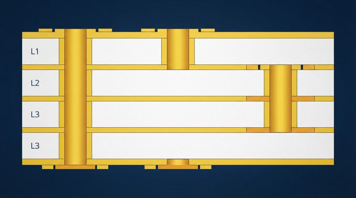
- Through-hole via — passes entirely through the board from top to bottom. Simplest to fabricate; visible on both outer layers.
- Blind via — connects an outer layer to one or more inner layers but does not exit the opposite side.
- Buried via — connects two or more inner layers without reaching either outer surface.
- Microvia — a laser-drilled via typically ≤ 150 µm in diameter, per IPC-2226. Used in HDI designs.
Typical Via Dimensions
| Parameter | Standard PCB (FR-4) | Ceramic PCB (LTCC / DPC) |
|---|---|---|
| Drill diameter | 0.2–0.5 mm | 0.1–0.3 mm (laser or punch) |
| Annular ring | ≥ 0.125 mm (per IPC-2221B) | Process-dependent; often ≥ 0.1 mm |
| Fill method | Electroplated copper or epoxy fill | Conductive paste (Ag, Au, or Cu) or plated copper |
Vias in Ceramic Substrates
On organic boards, vias are mechanically drilled and then electroplated. Ceramic substrates use different approaches. In LTCC (Low-Temperature Co-fired Ceramic), vias are punched or laser-cut into unfired “green” tape, filled with conductive paste, and co-fired with the ceramic. In DPC (Direct Plated Copper) substrates, vias are laser-drilled through the fired ceramic and then metallised by sputtering and electroplating.
Because ceramic is brittle, mechanical drilling risks cracking. Laser ablation with a CO₂ or UV laser is the standard method for fired substrates. Hole quality and sidewall roughness directly affect plating adhesion and via reliability.
Why Vias Matter
Beyond simple layer-to-layer routing, vias serve thermal and RF functions. Thermal vias — arrays of plated holes under a power device — conduct heat from a surface pad down to a heat-spreading layer or heatsink. In RF circuits, via fences surround transmission lines to suppress parasitic modes and provide a low-inductance ground return. Both applications are common on ceramic boards used in power electronics and microwave modules, where wire bonding connects die to the substrate’s top metallisation and vias carry signals or ground to the opposite side.
FAQ
Is a via the same as a plated through-hole?
A plated through-hole (PTH) is one type of via — specifically, one that passes all the way through the board. Blind and buried vias are also vias but are not through-holes.
Can ceramic PCBs have vias?
Yes. LTCC boards routinely include filled vias formed during the green-tape stage. DPC and thick-film ceramic substrates use laser-drilled and metallised vias. The minimum achievable diameter depends on the process and ceramic thickness.
What fills a via in an LTCC board?
LTCC vias are filled with a conductive paste — usually silver or silver-palladium — before the layers are laminated and co-fired. The paste sinters during firing to form a solid conductive plug.
For more ceramic PCB terms and definitions, browse the full ceramic PCB glossary.