Sintering is a thermal process in which compacted ceramic powder particles bond together at elevated temperature—below the material’s melting point—to form a dense, mechanically strong solid. Understanding this sintering definition is essential for anyone working with ceramic PCBs: sintering is the step that transforms a fragile “green” tape or pressed blank into a finished substrate with the dielectric strength, heat-transfer capability, and dimensional stability a circuit requires.
Sintering definition in ceramic PCB context
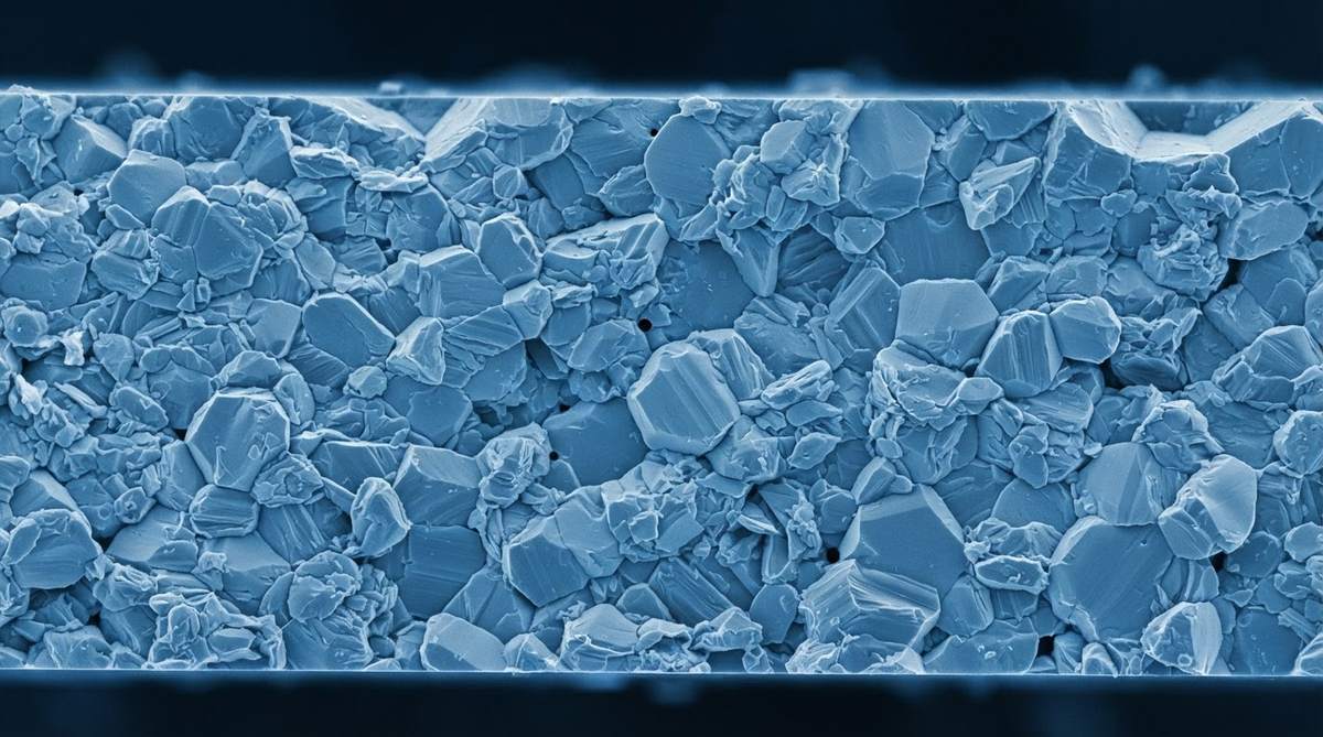
In ceramic PCB manufacturing, the sintering definition can be stated simply: heat-driven densification of a powder compact without reaching the liquid state of the base ceramic. During sintering, atoms migrate across particle boundaries. Pores between particles shrink and close, and the body contracts—typically 15–20 % linearly for alumina tapes. No liquid phase is needed in solid-state sintering, though some formulations add a glass flux to lower the required temperature (liquid-phase sintering).
The result is a polycrystalline ceramic whose density approaches 95–99.5 % of theoretical, depending on material grade and firing profile. This densification is what gives the finished ceramic substrate its mechanical strength, low porosity, and reliable electrical insulation.
Typical sintering temperatures by material
| Material | Sintering range | Process context |
|---|---|---|
| Al₂O₃ 96 % | 1 500–1 650 °C | HTCC co-firing |
| Al₂O₃ 99.6 % | 1 600–1 700 °C | HTCC / blank substrate |
| AlN | 1 750–1 900 °C | Requires N₂ atmosphere with Y₂O₃ sintering aid |
| LTCC glass-ceramic | 850–950 °C | Allows co-firing with Ag or Au conductors |
Values are representative ranges from CoorsTek and Kyocera technical datasheets. Confirm against the specific grade you specify.
Why sintering conditions matter for ceramic PCBs
Sintering conditions control grain size, residual porosity, and surface finish—all of which affect downstream steps. A substrate sintered to higher density exhibits better dielectric strength and lower thermal resistance. Under-sintered material is weaker and more porous, which can cause adhesion failures during thick-film printing or metallisation.
Shrinkage during sintering also determines final dimensional tolerance. HTCC processes must account for the ~17 % linear shrinkage of alumina tape; LTCC shrinkage is similar but occurs at a much lower temperature, which permits co-firing with lower-resistivity metals like silver.
Key properties affected by the sintering profile include:
- Density and porosity – higher sintering temperature or longer soak time yields fewer voids and stronger dielectric performance.
- Grain size – excessive temperature promotes grain growth, which can reduce flexural strength.
- Dimensional accuracy – inconsistent shrinkage across a panel causes warpage and tolerance drift.
- Surface roughness – finer grain structure after sintering produces smoother surfaces, improving metallisation adhesion.
Sintering vs. melting
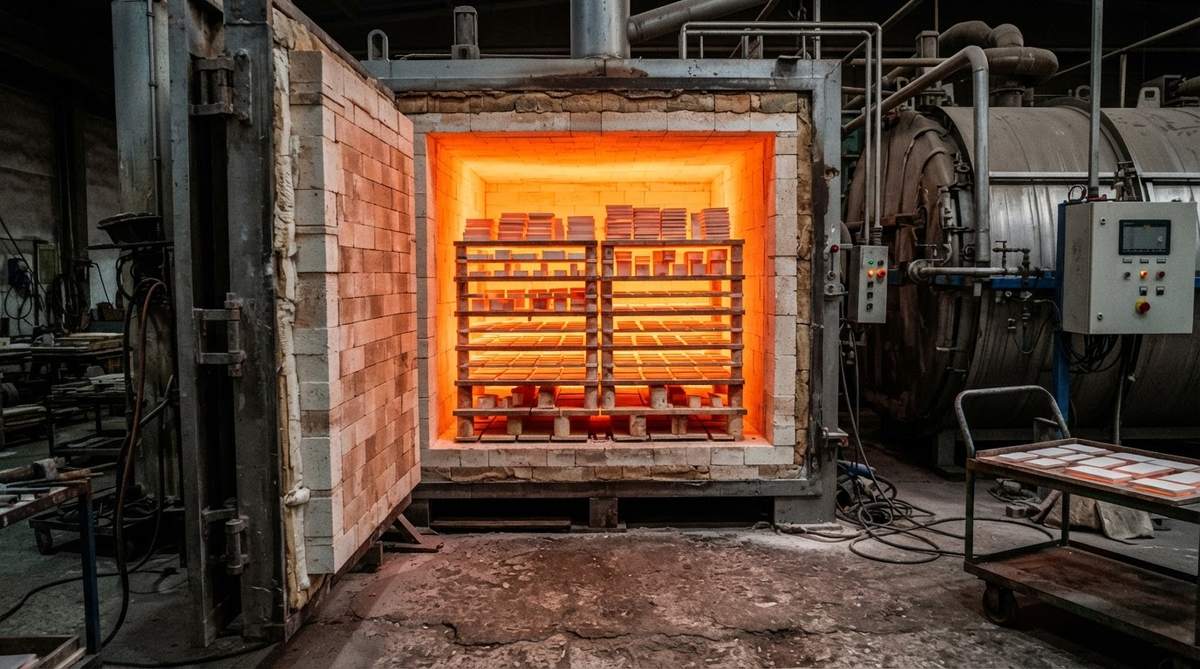
The sintering definition explicitly excludes melting. Alumina melts at approximately 2 072 °C, yet sinters effectively around 1 600 °C. This distinction is critical: the ceramic retains its crystalline microstructure rather than becoming amorphous, preserving the mechanical and thermal properties engineers rely on. If the material were melted and re-solidified, the controlled grain structure would be lost.
To see how sintering fits into the broader production sequence, read about the ceramic PCB manufacturing process.
Frequently asked questions
Is sintering the same as firing?
In ceramics, the terms are often used interchangeably. Strictly, “firing” refers to the entire thermal cycle (heating, soaking, cooling), while the sintering definition refers specifically to the densification mechanism that occurs during the high-temperature soak. For practical PCB work, treat them as synonyms.
Can sintering be reversed or redone?
No. Once a ceramic substrate has been sintered, the particle bonding is permanent. You cannot re-sinter a finished substrate to change its density or dimensions. Any corrections must happen before or during the green-tape stage.
Does sintering temperature affect which metals can be co-fired?
Yes, directly. HTCC sintering above 1 500 °C requires refractory metals like tungsten or molybdenum because copper and silver would melt. LTCC sintering at 850–950 °C is low enough to co-fire with silver or gold conductors, which offer much lower electrical resistivity.
Why does AlN need a nitrogen atmosphere for sintering?
Aluminum nitride oxidises readily above 700 °C in air, forming an alumina layer that degrades thermal conductivity. Sintering in a nitrogen atmosphere with yttria (Y₂O₃) as a sintering aid prevents oxidation and promotes full densification to achieve the 170–200 W/mK conductivity AlN is valued for.
For more ceramic PCB terminology, browse the full ceramic PCB glossary.