Introduction to Core PCB
A printed circuit board (PCB) is a fundamental component in modern electronic devices, serving as the foundation for mounting and connecting various electronic components. At the heart of a PCB lies its core, a critical element that provides structural stability and insulation between layers. In this article, we will delve into the concept of the core PCB, its composition, types, and the role it plays in the overall functionality of a printed circuit board.
What is a Core PCB?
A core PCB, also known as the substrate or base material, is the central layer of a printed circuit board. It is typically made of a non-conductive material, such as fiberglass or epoxy resin, which provides insulation between the conductive layers of the PCB. The core acts as a support structure for the copper traces, components, and other layers that make up the complete PCB Assembly.
Composition of a Core PCB
The most common material used for the core of a PCB is FR-4 (Flame Retardant 4), a composite material made of woven fiberglass cloth impregnated with an epoxy resin. FR-4 offers excellent electrical insulation properties, mechanical strength, and thermal stability, making it an ideal choice for a wide range of applications.
Other materials used for PCB cores include:
- Ceramic: Used in high-frequency and high-temperature applications
- Polyimide: Offers high heat resistance and flexibility
- Teflon: Provides low dielectric constant and high thermal stability
- Aluminum: Used for heat dissipation in high-power applications
Thickness of a Core PCB
The thickness of a core PCB can vary depending on the specific requirements of the application. Common thicknesses range from 0.2mm to 3.2mm, with 1.6mm being a standard thickness for many applications. The choice of thickness depends on factors such as the number of layers, the size and weight constraints of the device, and the required mechanical strength.

Types of Core PCBs
There are several types of core PCBs, each with its own unique characteristics and applications. Let’s explore some of the most common types:
Single-Sided Core PCB
A single-sided core PCB has conductive copper traces on only one side of the core material. This type of PCB is the simplest and most cost-effective option, suitable for basic electronic circuits with low complexity.
Double-Sided Core PCB
Double-sided core PCBs have copper traces on both sides of the core material, allowing for more complex circuit designs and higher component density. The two sides are connected through conductive vias, which are small holes drilled through the core and plated with copper.
Multi-Layer Core PCB
Multi-layer core PCBs consist of multiple layers of conductive copper traces separated by insulating core materials. The layers are interconnected through vias, enabling even more complex circuit designs and higher component density. Multi-layer PCBs are commonly used in advanced electronic devices, such as smartphones, computers, and medical equipment.

Manufacturing Process of Core PCBs
The manufacturing process of core PCBs involves several stages, each critical to ensuring the quality and reliability of the final product. Here’s a brief overview of the process:
-
Material Selection: The appropriate core material is selected based on the specific requirements of the application, such as FR-4, ceramic, or polyimide.
-
Cutting: The core material is cut to the desired size and shape using precise cutting tools.
-
Drilling: Holes are drilled through the core material to accommodate vias and component leads. The drilling process is typically carried out using computer-controlled drilling machines for accuracy and consistency.
-
Copper Deposition: A thin layer of copper is deposited onto the core material using a process called electroless Plating. This layer serves as a conductive base for the subsequent etching process.
-
Photoresist Application: A photoresist layer is applied to the copper-coated core material and then exposed to UV light through a photomask, which contains the desired circuit pattern.
-
Etching: The exposed copper areas are etched away using a chemical solution, leaving behind the desired copper traces that form the circuit pattern.
-
Resist Removal: The remaining photoresist is removed, revealing the final copper circuit pattern on the core material.
-
Inspection: The core PCB undergoes a thorough inspection to ensure that the circuit pattern is accurate and free of defects.
-
Lamination (for multi-layer PCBs): Multiple core PCBs are laminated together with insulating layers in between to form a multi-layer PCB.
-
Surface Finishing: The core PCB may undergo additional surface finishing processes, such as solder mask application and silkscreen printing, to protect the copper traces and improve solderability.

Advantages of Core PCBs
Core PCBs offer several advantages that make them an essential component in modern electronic devices:
-
Structural Stability: The core material provides a stable foundation for the PCB, ensuring that the components and traces remain securely in place.
-
Insulation: The non-conductive nature of the core material offers excellent electrical insulation between the conductive layers, preventing short circuits and signal interference.
-
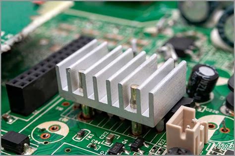
Heat Dissipation: Some core materials, such as aluminum, can help dissipate heat generated by electronic components, improving the overall thermal management of the device.
-
Customization: Core PCBs can be customized to suit specific application requirements, such as thickness, material selection, and circuit design.
-
Cost-Effective: Core PCBs are a cost-effective solution for a wide range of electronic applications, particularly when compared to other alternatives like point-to-point wiring.
Applications of Core PCBs
Core PCBs find applications in a diverse range of industries and electronic devices, including:
- Consumer Electronics: Smartphones, tablets, laptops, and wearables
- Automotive: Engine control units, infotainment systems, and sensors
- Industrial: Process control systems, automation equipment, and power electronics
- Medical: Diagnostic equipment, monitoring devices, and implantable devices
- Aerospace and Defense: Avionics, communication systems, and radar equipment
Frequently Asked Questions (FAQ)
-
What is the difference between a core PCB and a regular PCB?
A core PCB refers specifically to the central insulating layer of a printed circuit board, while a regular PCB is the complete assembly, including the core, copper traces, and components. -
Can a core PCB be used without additional layers?
Yes, a single-sided core PCB can be used for simple electronic circuits that do not require complex routing or high component density. -
What is the most common material used for the core of a PCB?
FR-4, a composite material made of woven fiberglass cloth impregnated with an epoxy resin, is the most common material used for PCB cores. -
How does the thickness of a core PCB affect its performance?
The thickness of a core PCB can influence its mechanical strength, thermal management, and the overall size and weight of the device. Thicker cores offer better stability and heat dissipation but may increase the size and weight of the PCB. -
Are core PCBs environmentally friendly?
The environmental impact of core PCBs depends on the materials used and the manufacturing processes employed. Some manufacturers use eco-friendly materials and adopt sustainable practices to minimize the environmental footprint of PCB production.
Conclusion
The core of a PCB is a critical component that provides the foundation for the entire printed Circuit board assembly. It offers structural stability, insulation, and customization options to suit a wide range of electronic applications. Understanding the composition, types, and manufacturing process of core PCBs is essential for designers, engineers, and manufacturers working in the electronics industry.
As technology continues to advance, the demand for high-quality, reliable, and cost-effective core PCBs will only grow. By staying informed about the latest developments and best practices in core PCB design and manufacturing, professionals can ensure that they are well-equipped to meet the evolving needs of the industry.
| Core PCB Material | Advantages | Disadvantages |
|---|---|---|
| FR-4 | – Excellent insulation properties – Mechanical strength – Thermal stability |
– Limited high-frequency performance |
| Ceramic | – High-frequency performance – High-temperature resistance |
– Brittle – Expensive |
| Polyimide | – High heat resistance – Flexibility |
– Expensive – Difficult to process |
| Teflon | – Low dielectric constant – High thermal stability |
– Expensive – Difficult to bond |
| Aluminum | – Excellent heat dissipation – Mechanical strength |
– Requires insulation layer – Limited flexibility |
In summary, core PCBs are the backbone of modern electronic devices, providing the necessary structure, insulation, and connectivity for complex circuit designs. By understanding the intricacies of core PCBs and their role in the overall PCB assembly, professionals can make informed decisions when designing and manufacturing electronic products that meet the highest standards of quality and performance.


Leave a Reply