Introduction to PCB Inner Layers
Printed Circuit Boards (PCBs) are essential components in modern electronics, providing a platform for interconnecting various electronic components. While the outer layers of a PCB are readily visible, it’s the inner layers that hold the key to the board’s functionality and performance. In this article, we will dive deep into the world of PCB inner layers, exploring their composition, manufacturing process, and their crucial role in the overall functionality of a PCB.
What are PCB Inner Layers?
PCB inner layers, also known as internal layers, are the conductive layers sandwiched between the top and bottom layers of a multi-layer PCB. These layers are responsible for carrying signals and power between components on the board. The number of inner layers in a PCB can vary depending on the complexity and requirements of the design, ranging from just a few to dozens in high-density boards.
Composition of Inner PCB Layers
The inner layers of a PCB are typically made of a thin layer of Copper Foil laminated onto a dielectrIC Substrate material, such as FR-4. The copper foil thickness can vary depending on the requirements of the design, with common thicknesses ranging from 0.5 oz to 2 oz per square foot. The dielectric substrate provides insulation between the conductive layers, preventing short circuits and signal interference.
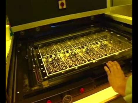
Manufacturing Process of PCB Inner Layers
Step 1: Lamination
The first step in manufacturing PCB inner layers is the lamination process. The copper foil is laminated onto the dielectric substrate using heat and pressure. This process ensures a strong bond between the copper and the substrate, creating a stable base for the subsequent steps.
Step 2: Drilling
Once the lamination is complete, the next step is to drill holes through the inner layers. These holes, known as vias, allow for electrical connections between the different layers of the PCB. The drilling process is typically done using high-speed CNC machines, ensuring precise and accurate hole placement.
Step 3: Patterning
After drilling, the inner layers undergo a patterning process to create the desired circuit pattern. This is typically done using a photolithography process, where a light-sensitive resist is applied to the copper surface, and then exposed to light through a patterned mask. The exposed areas of the resist are then removed, leaving behind a pattern of exposed copper.
Step 4: Etching
The exposed copper is then etched away using a chemical solution, typically an acidic mixture of hydrogen peroxide and sulfuric acid. This process removes the unwanted copper, leaving behind the desired circuit pattern on the inner layer.
Step 5: Inspection and Testing
After etching, the inner layers undergo a thorough inspection and testing process to ensure the accuracy and quality of the circuit pattern. This includes visual inspections, as well as electrical tests to verify the continuity and insulation of the circuits.

Role of Inner PCB Layers in PCB Functionality
Signal Integrity
One of the primary roles of inner PCB layers is to maintain signal integrity throughout the board. By providing a controlled impedance environment for the signals to travel through, inner layers help to minimize signal distortion and interference. This is particularly important in high-speed designs, where signal integrity is critical to the overall performance of the board.
Power Distribution
Inner layers also play a crucial role in power distribution within a PCB. By dedicating specific layers to power and ground planes, designers can ensure a stable and reliable power supply to all components on the board. This helps to minimize voltage drops and reduce electromagnetic interference (EMI) that can negatively impact the performance of the circuit.
Electromagnetic Compatibility (EMC)
Inner layers can also be used to improve the electromagnetic compatibility (EMC) of a PCB. By strategically placing ground planes and power planes, designers can create a shielding effect that helps to reduce EMI and improve the overall EMC performance of the board. This is particularly important in applications where the PCB is exposed to high levels of electromagnetic interference, such as in automotive or aerospace systems.
Thermal Management
In addition to their electrical functions, inner layers can also contribute to the thermal management of a PCB. By providing additional copper for heat dissipation, inner layers can help to spread heat more evenly across the board, reducing hot spots and improving overall thermal performance. This is particularly important in high-power applications, where effective thermal management is critical to the reliability and longevity of the board.

Types of Inner PCB Layers
Signal Layers
Signal layers are the most common type of inner PCB layer, responsible for carrying signals between components on the board. These layers are typically designed with controlled impedance characteristics to maintain signal integrity and minimize distortion.
Power and Ground Layers
Power and ground layers are dedicated to providing a stable and reliable power supply to the components on the board. These layers are typically designed as solid planes, providing a low-impedance path for current to flow.
Split Planes
Split planes are a type of inner layer that combines both power and ground planes on the same layer. This design technique is often used to save space and reduce the overall layer count of the board. However, split planes require careful design considerations to avoid signal integrity issues and ensure proper power distribution.

Design Considerations for Inner PCB Layers
Layer Stackup
The layer stackup is a critical design consideration for inner PCB layers. The stackup defines the arrangement and order of the layers within the board, as well as the spacing between them. A well-designed stackup can help to optimize signal integrity, power distribution, and thermal performance, while a poorly designed stackup can lead to a range of issues, including signal reflections, crosstalk, and EMI.
Via Design
Via design is another important consideration for inner PCB layers. Vias are the holes drilled through the layers to provide electrical connections between them. The size, spacing, and placement of vias can have a significant impact on signal integrity and manufacturability. Designers must carefully consider via design to ensure optimal performance and reliability.
Copper Thickness
The thickness of the copper on the inner layers is another important design consideration. Thicker copper can provide better current carrying capacity and improved thermal performance, but it can also increase the overall cost and weight of the board. Designers must balance these factors to select the appropriate copper thickness for their specific application.
Material Selection
The choice of dielectric substrate material is another critical design consideration for inner PCB layers. Different materials have different electrical and thermal properties, as well as varying costs and manufacturing considerations. Designers must carefully select the appropriate material based on the specific requirements of their application, taking into account factors such as Dielectric Constant, Loss Tangent, and thermal conductivity.
Frequently Asked Questions (FAQ)
1. What is the purpose of inner layers in a PCB?
Inner layers in a PCB serve multiple purposes, including carrying signals between components, providing power distribution, improving electromagnetic compatibility, and contributing to thermal management.
2. How many inner layers can a PCB have?
The number of inner layers in a PCB can vary depending on the complexity and requirements of the design. Simple boards may have just a few inner layers, while high-density boards can have dozens of layers.
3. What materials are used for inner PCB layers?
Inner PCB layers are typically made of a thin layer of copper foil laminated onto a dielectric substrate material, such as FR-4. The specific materials used can vary depending on the requirements of the application.
4. How are inner PCB layers manufactured?
The manufacturing process for inner PCB layers involves several steps, including lamination, drilling, patterning, etching, and inspection. Each step plays a critical role in ensuring the accuracy and quality of the final product.
5. What design considerations are important for inner PCB layers?
Key design considerations for inner PCB layers include layer stackup, via design, copper thickness, and material selection. Each of these factors can have a significant impact on the performance, reliability, and manufacturability of the board.
Conclusion
Inner PCB layers are a critical component of modern printed circuit boards, providing the necessary connectivity and functionality for today’s complex electronic systems. Understanding the composition, manufacturing process, and role of inner layers is essential for designers looking to create high-performance, reliable PCBs.
By carefully considering factors such as layer stackup, via design, copper thickness, and material selection, designers can optimize the performance and manufacturability of their boards, ensuring the best possible outcomes for their specific applications.
As PCB technology continues to evolve, the importance of inner layers will only continue to grow. By staying up-to-date with the latest advancements and best practices in inner layer design, engineers and manufacturers can stay ahead of the curve, delivering cutting-edge solutions for a wide range of industries and applications.
| Layer Type | Purpose | Design Considerations |
|---|---|---|
| Signal Layers | Carry signals between components | Controlled impedance, signal integrity |
| Power and Ground Layers | Provide stable power distribution | Low impedance, EMI reduction |
| Split Planes | Combine power and ground on same layer | Space saving, signal integrity |
In summary, the inner layers of a PCB play a vital role in the overall functionality and performance of the board. By understanding the intricacies of inner layer design and manufacturing, engineers and manufacturers can create high-quality, reliable PCBs that meet the demands of today’s complex electronic systems.


Leave a Reply