You can typically reduce ceramic PCB cost by 20–50% without changing the circuit’s electrical or thermal performance. The biggest savings come from material grade selection, panel utilization, and tolerance relaxation—three levers that most engineers never revisit after the prototype phase. Below are nine methods, ranked roughly by impact, with numbers you can plug into your own project.
Key Takeaways
- Switching from 99.6% alumina to 96% alumina cuts substrate cost by 30–40% and is sufficient for most designs below 50 W/cm².
- Optimizing panel utilization from 60% to 85% can reduce per-unit cost by roughly 25%, because you pay for the whole panel.
- Relaxing position tolerance from ±25 µm to ±50 µm often moves a job from thin-film to thick-film or DPC processing, halving metallization cost.
- Combining prototype and production orders into a single qualified run eliminates duplicate NRE tooling charges.
- A complete RFQ package—Gerbers, stackup, material spec, quantity schedule—gets you a faster, lower quote than an incomplete one.
1. Choose the Right Ceramic Grade—Not the Best One
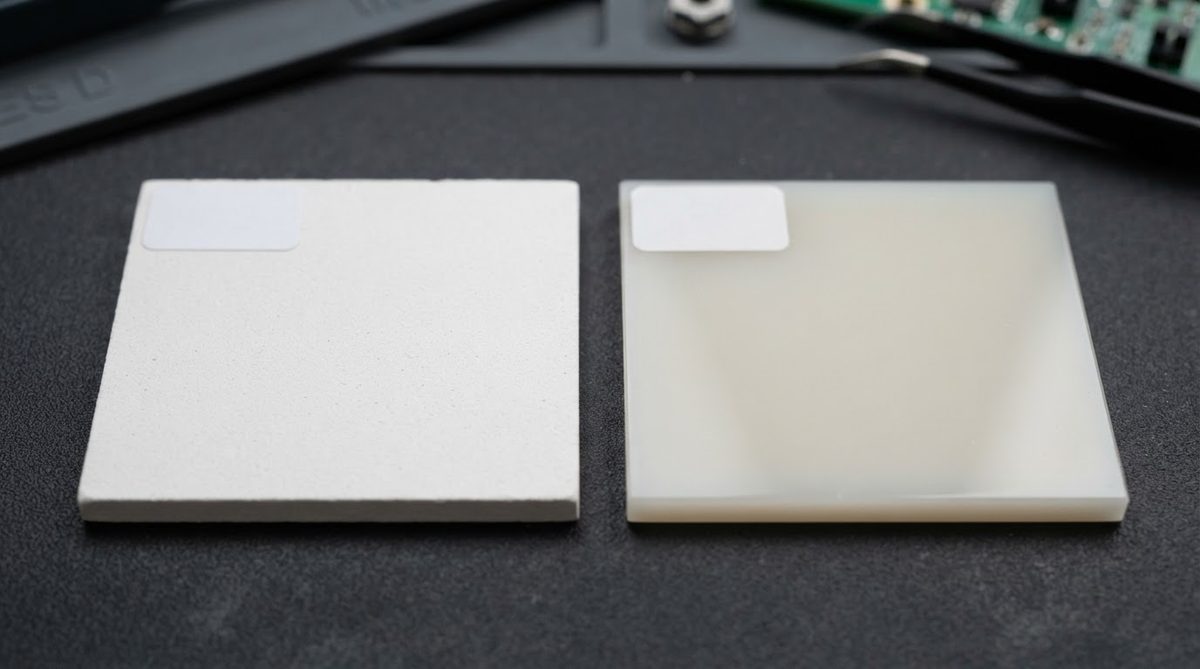
Material is the single largest cost driver. Aluminum nitride (AlN) substrates cost 3–5× more per unit area than 96% alumina (Al₂O₃). Silicon nitride (Si₃N₄) is even more expensive. Many engineers default to AlN for its 170–200 W/m·K thermal conductivity when 96% alumina at 24–28 W/m·K would keep junction temperatures within spec. For a deeper look at Si₃N₄ substrate cost factors, see our dedicated analysis.
Decision rule: Calculate the thermal resistance from junction to heatsink. If the substrate contribution is less than 20% of the total thermal path resistance, the cheaper grade will work. Upgrading the material won’t meaningfully lower Tj.
Worked Example: Alumina vs. AlN
A 10 × 10 mm substrate, 0.635 mm thick, dissipating 15 W:
| Parameter | 96% Al₂O₃ | AlN | Unit |
|---|---|---|---|
| Thermal conductivity (k) | 25 | 180 | W/m·K |
| Substrate Rth (t / k·A) | 2.54 | 0.35 | °C/W |
| ΔT across substrate at 15 W | 38.1 | 5.3 | °C |
| Typical substrate cost (qty 500) | ~$0.80 | ~$3.20 | per unit |
If your thermal budget allows a 38 °C rise across the substrate, alumina saves roughly $1,200 on a 500-piece run. If it doesn’t, AlN is justified—but verify with the actual numbers, not intuition.
2. Maximize Panel Utilization
Ceramic substrates are processed as panels. You pay for the full panel regardless of how many unit boards you fit on it. Poor utilization wastes material and furnace time.
- Work with your manufacturer to adjust board outline or routing channels so more units nest per panel.
- A 1 mm reduction in board-to-board spacing on a 114 × 114 mm panel can add 2–4 extra units, cutting per-piece cost by 5–10%.
- If your design allows rotation, alternating orientation can improve nesting on rectangular substrates.
Ask your supplier for a panelization drawing before locking the board outline. This is free and takes one email.
3. Relax Tolerances You Don’t Actually Need
Tight tolerances push jobs toward more expensive processes. A ±25 µm line/space spec requires thin-film sputtering and photolithography. A ±50 µm spec can often be met with DPC (direct plated copper) or thick-film screen printing, which cost significantly less per layer.
Review your design: are those 75 µm traces driven by the circuit, or are they just carried over from an IC-substrate reference design? Most power and sensor circuits function fine at 100–150 µm trace/space. For a full breakdown of how these choices affect pricing, see the ceramic PCB cost breakdown.
4. Standardize Substrate Thickness
Common alumina thicknesses—0.25, 0.38, 0.50, 0.635, and 1.0 mm—are stocked by substrate manufacturers and ship faster with lower minimums. Non-standard thicknesses (e.g., 0.45 mm) require custom lapping or pressing, adding $200–$600 in NRE and 1–2 weeks of lead time. Unless your mechanical stackup demands it, pick a standard gauge.
5. Consolidate Orders and Plan Quantities
Ceramic PCB pricing has steep quantity breaks. A common pattern:
| Quantity | Typical per-unit cost index |
|---|---|
| 10 pcs (prototype) | 1.00× (baseline) |
| 100 pcs | 0.45–0.55× |
| 500 pcs | 0.30–0.40× |
| 5,000 pcs | 0.18–0.25× |
If you know you’ll need 500 units over six months, ordering them in one run—even if you stagger delivery—avoids paying setup and screen/mask charges twice. Discuss blanket orders with your supplier.
6. Simplify the Surface Finish
ENIG and ENEPIG add $0.10–$0.30 per cm² over bare fired metallization. If your assembly process allows it, immersion silver or even bare gold thick-film pads may be sufficient. For wire-bond pads, electrolytic gold is unavoidable, but limiting it to the bond-pad area (selective plating) instead of full-panel plating saves gold and chemistry cost.
7. Reduce Via and Through-Hole Count
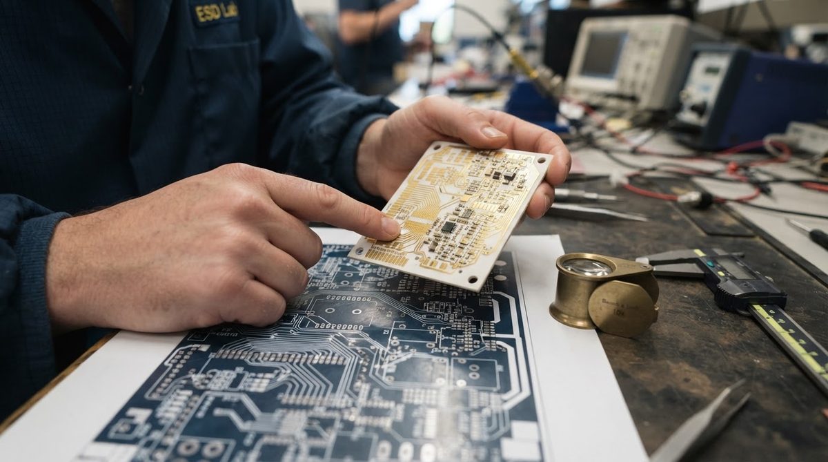
Vias in ceramic substrates—especially filled vias in HTCC or LTCC—require individual punching, filling with tungsten or molybdenum paste, and co-firing. Each via adds cost. If your design has ground vias on a 0.5 mm pitch “because that’s what the layout tool defaulted to,” consider whether a 1.0 mm pitch or a solid ground plane on the opposite side achieves the same return-path impedance. Fewer vias also improve yield, which lowers cost indirectly.
8. Provide a Complete RFQ Package
Incomplete quote requests get padded with worst-case assumptions. A supplier who doesn’t know your tolerance requirement will quote the tightest one they offer. Send Gerbers, a stackup drawing, material and finish specs, quantity with annual forecast, and any compliance requirements. Download our ceramic PCB RFQ template to make sure nothing is missing, or see what to send for an accurate quote.
Enter your board dimensions, material, and quantity below to get a ballpark cost estimate before you submit a formal RFQ.
[pcb_calc type=”pcb-quote”]
9. Design for Yield
Ceramic is brittle. Boards with sharp internal corners, narrow necks, or slots near the edge are more likely to crack during singulation or handling. Every scrapped unit raises the effective cost of the good ones. Use ≥0.5 mm corner radii, keep slots at least 2 mm from the board edge, and avoid L-shaped or U-shaped outlines where a simple rectangle would work. These are free changes that can improve yield by 5–15% on complex geometries.
When Ceramic Is Not the Right Call
If your primary motivation is cost, and your thermal or frequency requirements can be met by another substrate, ceramic may not be justified:
- Metal-core PCBs (MCPCBs) handle 1–4 W/m·K thermal conductivity at a fraction of ceramic cost. Sufficient for many LED and low-density power designs.
- High-Tg FR-4 or polyimide survive up to 260–280 °C peak reflow and cost 5–10× less per unit area than alumina. If your operating temperature stays below 150 °C and your frequency is under 3 GHz, FR-4 often wins.
- IMS (insulated metal substrate) is another middle ground for single-sided thermal designs.
Ceramic earns its premium when you need continuous operation above 300 °C, dielectric stability at mmWave frequencies, CTE matching to GaN or SiC die, or hermeticity. For application-specific cost guidance, see our pages on SiC power module PCB cost and sensor and MEMS substrate cost.
Frequently Asked Questions
Does 96% alumina perform worse than 99.6% alumina electrically?
For most circuits, no. Both grades have a dielectric constant of roughly 9.0–9.9 at 1 MHz (per CoorsTek ADS-96R and ADS-996 datasheets). The 99.6% grade offers slightly lower dielectric loss and higher flexural strength (400 MPa vs. 340 MPa, ASTM C1161), but the electrical difference is negligible below 20 GHz for typical trace geometries.
Can I mix ceramic and FR-4 in the same product to save money?
Yes. A common approach mounts a small ceramic sub-board (carrying the high-power or high-frequency section) onto a larger FR-4 motherboard. This limits ceramic usage to where it’s needed and keeps total BOM cost down. The interconnect is usually wire bond or solder-attach, depending on the frequency.
How much does NRE tooling typically cost for ceramic PCBs?
Screen printing screens run $50–$200 each. Photo-masks for DPC or thin-film run $150–$500 per layer. Laser tooling for via drilling or singulation is often a one-time programming charge of $100–$300. These are amortized across the order, so larger quantities dilute NRE to near zero per unit.
Is it cheaper to order ceramic PCBs as bare substrates and do metallization in-house?
Rarely. In-house metallization requires vacuum deposition or screen-printing equipment, a controlled atmosphere furnace, and photolithography capability. Unless you already run these processes for another product line, outsourcing the complete circuit to a ceramic PCB manufacturer is almost always cheaper and faster.
Do lead times affect cost?
Yes. Expedited orders (under 5 business days) typically carry a 30–80% surcharge because they disrupt production scheduling. Standard lead times of 2–3 weeks avoid this premium entirely. Planning ahead is the simplest cost reduction available.
Next Step
Pick two or three of the methods above that apply to your current design, update your spec, and request a revised quote. If you’re starting fresh, use our RFQ template to make sure your first quote is accurate. For questions about material grade selection or panelization, contact our engineering team directly.