Choosing the wrong PCB substrate for a high-power or high-frequency application is one of the costliest mistakes an engineer can make. Alumina PCB (Al2O3), aluminum nitride (AlN), and other ceramic circuit board materials solve thermal, electrical, and mechanical problems that standard FR4 simply cannot handle. This guide breaks down every critical property, comparison, and selection criterion so you can specify the right ceramic substrate with confidence.
What Is an Alumina PCB and Why Does It Matter
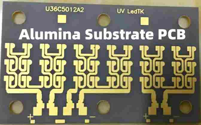
An alumina PCB — also called an Al2O3 ceramic PCB or aluminum oxide PCB — uses a fired ceramic substrate instead of the glass-epoxy laminate found in conventional boards. The substrate is composed primarily of aluminum oxide (Al2O3), typically at purities of 96%, 99%, or 99.6%.
The ceramic base delivers properties that polymer laminates cannot match: stable dielectric characteristics across a wide temperature range, excellent electrical insulation even at elevated operating temperatures, and a thermal conductivity several times higher than FR4. These traits make alumina PCBs the default choice in power modules, RF/microwave assemblies, LED lighting arrays, automotive sensors, and aerospace electronics.
Because ceramic does not absorb moisture and does not burn, alumina circuit boards also satisfy demanding reliability and safety requirements in medical devices and industrial controls.
Al2O3 vs AlN: Choosing Between the Two Main Ceramic PCB Materials
The two dominant ceramic substrate materials are aluminum oxide (Al2O3) and aluminum nitride (AlN). Understanding their differences before you specify a board saves significant cost and rework time.
Aluminum Oxide (Al2O3) — The Workhorse Ceramic
96% alumina is the industry standard grade, balancing performance and cost. It offers:
- Thermal conductivity: 20–24 W/(m·K) for 96% grade; up to 35 W/(m·K) for 99.6%
- Dielectric constant (1 MHz): approximately 9.8
- Volume resistivity: >10¹⁴ Ω·cm
- Maximum continuous operating temperature: ~350 °C (short-term excursions to 1,000 °C)
- Coefficient of thermal expansion (CTE): 6.7–7.1 ppm/°C — a close match to silicon and GaAs
The higher the alumina purity, the smoother the surface finish, the lower the dielectric loss, and the better the thermal conductivity — but unit cost rises accordingly.
Aluminum Nitride (AlN) — The High-Performance Option
AlN PCB substrates command a price premium but deliver thermal conductivity in the range of 140–180 W/(m·K), roughly 6–8× that of standard alumina. Key characteristics include:
- Dielectric constant: ~8.8 — lower than Al2O3, beneficial for high-frequency designs
- CTE: ~4.6 ppm/°C — exceptionally close to silicon, reducing solder fatigue in flip-chip assemblies
- Flexural strength: 280–350 MPa, somewhat lower than alumina
- Toxicity note: AlN powder requires careful handling; finished sintered boards are safe
AlN is the substrate of choice for high-brightness LED modules, GaN power devices, and laser diode packages where heat flux densities exceed what alumina can dissipate without thermal throttling.
Comparison Table: Al2O3 vs AlN vs FR4
| Property | 96% Al2O3 | 99.6% Al2O3 | AlN | FR4 |
|---|---|---|---|---|
| Thermal conductivity (W/m·K) | 20–24 | 30–35 | 140–180 | 0.3–0.4 |
| Dielectric constant (1 GHz) | ~9.8 | ~9.9 | ~8.8 | ~4.5 |
| CTE (ppm/°C) | 6.7–7.1 | 6.8 | 4.5–4.7 | 14–17 |
| Max operating temp (°C) | 350+ | 350+ | 350+ | ~130 |
| Relative cost | Low | Medium | High | Very low |
| Machinability | Laser/diamond | Laser/diamond | Laser/diamond | Standard drill |
[EXTERNAL LINK: IPC standards for ceramic substrate design → https://www.ipc.org]
Key Manufacturing Processes for Ceramic PCBs
Ceramic PCB fabrication differs substantially from standard PCB processing. The three main metallization and forming technologies are:
- DBC (Direct Bonded Copper) — Copper foil is bonded directly to the ceramic at high temperature, forming a eutectic Cu-CuO bond. DBC on alumina is common in IGBT and power module bases. Copper thickness ranges from 127 µm to 400 µm, enabling high current-carrying capacity.
- AMB (Active Metal Brazing) — A silver-copper-titanium braze alloy bonds copper to the ceramic. AMB achieves stronger adhesion than DBC and is preferred for AlN substrates where the DBC process is less straightforward. AMB can achieve copper layers up to 600 µm.
- Thick Film / LTCC — Conductive pastes (silver, gold, or platinum-gold) are screen-printed onto the ceramic and fired at 850–1,000 °C. LTCC (Low-Temperature Co-fired Ceramic) allows multilayer construction with buried passive components. Thick-film alumina PCBs are widely used in hybrid integrated circuits and sensor modules.
[INTERNAL LINK: thick-film alumina substrate applications → /thick-film-ceramic-pcb]
The choice of metallization method determines trace resolution, current capacity, thermal cycling reliability, and ultimately cost.
Design Rules and Tolerances Unique to Ceramic PCBs
Engineers transitioning from FR4 to alumina or AlN substrates must account for several design rule differences:
- Minimum trace width/spacing: Typically 75–100 µm for thick-film; 100–150 µm for DBC — coarser than advanced organic PCBs but sufficient for most power applications.
- Via technology: Ceramic boards use laser-drilled or punched vias filled with conductive paste before firing; blind and buried vias are possible in LTCC.
- Panelization: Alumina panels are scribed (laser or mechanical) then broken after component assembly; sharp edges require careful handling.
- Surface finish: Al2O3 surface roughness (Ra) is typically 0.4–0.8 µm for 96% grade; higher-purity grades reach Ra < 0.2 µm, which improves wire bonding yield.
- Warpage: Ceramic substrates are dimensionally stable, but large panels (>100 mm) can exhibit bow of 0.1–0.3%; specify flatness requirements explicitly.
Thermal simulation before layout is strongly recommended. Tools like ANSYS Icepak or Simcenter Flotherm help validate junction temperatures before the first prototype is ordered.
Primary Applications of Alumina and AlN PCBs
Understanding where ceramic PCBs are deployed clarifies whether your application genuinely warrants the cost premium.
Power Electronics and EV Inverters
IGBT modules and SiC MOSFET power stages generate intense, localized heat. DBC alumina — and increasingly DBC AlN — substrates sit directly beneath the die, conducting heat to the baseplate. EV traction inverters, solar inverters, and industrial motor drives are the largest volume markets for ceramic PCB substrates globally.
High-Frequency RF and Microwave Assemblies
Low dielectric loss (tan δ < 0.0003 for 99.6% alumina at 10 GHz) makes aluminum oxide PCBs suitable for microwave filters, patch antennas, and radar front-end modules. At millimeter-wave frequencies above 30 GHz, AlN’s slightly lower dielectric constant and loss tangent give it an edge over standard alumina.
LED and Photonics Modules
High-brightness LEDs generate roughly 70% of their input power as heat. An alumina PCB substrate under the LED array dissipates that heat faster than metal-core PCBs in many geometries, while also providing a stable optical reference surface. COB (chip-on-board) LED modules for automotive headlamps and industrial luminaires are a fast-growing segment.
Medical and Aerospace Electronics
Hermetic sealing compatibility, zero outgassing, gamma-radiation resistance, and long-term dimensional stability make ceramic PCBs preferred in implantable devices, satellite transponders, and avionics black boxes.
[INTERNAL LINK: ceramic PCB for medical devices → /ceramic-pcb-medical-applications]
How to Select the Right Alumina PCB Grade for Your Project
Use this decision framework when specifying a ceramic substrate:
- Identify peak heat flux density. If your power device dissipates more than 50 W/cm², standard 96% alumina may be insufficient; evaluate 99.6% Al2O3 or AlN.
- Check CTE compatibility. If die-attach or solder reliability is critical over wide temperature swings (−55 °C to +150 °C), AlN’s 4.6 ppm/°C CTE better matches silicon than alumina’s 6.9 ppm/°C.
- Assess frequency requirements. Above 10 GHz, specify 99.6% alumina or AlN to keep dielectric losses acceptably low.
- Define metallization current rating. Standard thick-film silver conductors carry ~5 A/mm of width; DBC copper handles 10–20× more.
- Factor manufacturing volume. Thick-film alumina is cost-effective at low-to-medium volumes. DBC and AMB processes have higher tooling costs but become competitive above roughly 500–1,000 pieces per run.
- Confirm supplier qualification. Look for ISO 9001 certification, IATF 16949 for automotive programs, and IPC-A-610 inspection capability.
Sourcing Alumina PCBs: What to Look for in a Manufacturer
The ceramic PCB supply chain is more concentrated than the FR4 market. Most substrate-grade alumina comes from Japan, Germany, and China. When evaluating suppliers:
- Request material certifications confirming Al2O3 purity and thermal conductivity measured by the laser flash method (ASTM E1461).
- Ask for cross-sectional SEM images or X-ray fluorescence (XRF) data for metallization adhesion verification.
- Confirm minimum order quantities (MOQs) — prototyping MOQs for ceramic boards are typically 5–20 pieces, not single units.
- Evaluate lead time realism. Standard thick-film alumina PCBs typically require 3–5 weeks; DBC and AMB substrates often need 6–10 weeks for first articles.
- Verify thermal cycling test data if the application involves repeated power cycling (IEC 60749-34 or equivalent).
[EXTERNAL LINK: ASTM thermal conductivity test methods → https://www.astm.org]
Conclusion
Alumina PCB and AlN ceramic substrates fill a performance gap that no organic laminate can close — combining high thermal conductivity, outstanding electrical insulation, CTE compatibility with semiconductor dies, and long-term stability at elevated temperatures. Whether you need a 96% Al2O3 board for a cost-sensitive power supply, a 99.6% alumina substrate for a microwave module, or an AlN ceramic PCB for a next-generation GaN power stage, the right material selection starts with a clear understanding of heat flux, frequency, CTE, metallization method, and volume.
Our engineering team specializes in alumina and AlN PCB design review, prototyping, and production. Contact us to discuss your thermal and electrical requirements and receive a tailored substrate recommendation.
Frequently Asked Questions
What is the difference between an alumina PCB and a standard aluminum PCB?
An alumina PCB uses a sintered aluminum oxide (Al2O3) ceramic substrate that is an excellent electrical insulator and has a thermal conductivity of 20–35 W/(m·K). A standard aluminum PCB (metal-core PCB) uses an aluminum metal base with a thin dielectric polymer layer; it conducts electricity and relies on the polymer layer for insulation. Alumina ceramic PCBs handle higher temperatures, offer better electrical isolation, and are more suitable for die-attach and RF applications.
Is an AlN PCB worth the extra cost over alumina?
AlN PCBs cost roughly 3–5× more than comparable alumina substrates. The premium is justified when heat flux density exceeds ~50–80 W/cm², when CTE matching to silicon is critical for long-term solder reliability, or when operating frequencies above 10 GHz require lower dielectric loss. For general-purpose power modules below those thresholds, 96% Al2O3 is the economical choice.
Can alumina ceramic PCBs be used with standard SMT assembly processes?
Yes, with modifications. Ceramic PCBs are compatible with standard solder paste, reflow ovens, and wire bonding equipment. The main adjustments involve using solder alloys and paste formulations suited to the surface finish (typically ENIG or silver thick-film), ensuring reflow profiles respect the lower thermal mass of ceramic compared to FR4, and using handling fixtures to prevent edge chipping during pick-and-place.
What purity level of Al2O3 should I specify for microwave circuits?
For circuits operating below 6 GHz, 96% alumina is generally adequate. For applications in the 6–30 GHz range, 99.6% alumina significantly reduces dielectric loss and surface roughness, improving insertion loss. Above 30 GHz, AlN or specialized low-loss ceramics (e.g., BeO — note beryllium oxide toxicity — or CVD diamond for extreme cases) are considered.
How are holes and cutouts made in alumina PCBs?
Alumina is too hard for conventional mechanical drilling at production scale. The standard methods are laser machining (CO₂ or Nd:YAG lasers for green-state ceramic, ultrashort-pulse lasers for fired alumina) and ultrasonic drilling for larger holes. Scribing lines for panel singulation are laser-cut before or after metallization. Tolerances of ±0.05–0.1 mm are achievable; tighter tolerances require grinding or laser trimming.


Leave a Reply