What is Solder Mask?
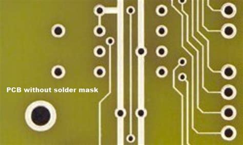
Solder mask, also known as solder resist or solder stop, is a thin layer of polymer material applied to the surface of a PCB. It is typically green in color but can also be found in other colors such as red, blue, or black. The primary purpose of solder mask is to protect the copper traces on the PCB from oxidation, corrosion, and accidental short-circuiting during the soldering process.
Composition of Solder Mask
Solder mask is composed of a mixture of epoxy resins, hardeners, fillers, and pigments. The specific composition may vary depending on the manufacturer and the intended application of the PCB. Some common types of solder mask include:
- Liquid Photoimageable Solder Mask (LPSM)
- Dry Film Solder Mask (DFSM)
- Liquid Photoimageable Dry Film (LPI-DF)
Each type has its own advantages and disadvantages in terms of ease of application, durability, and cost.
Functions of Solder Mask in PCB
1. Protection against Oxidation and Corrosion
One of the primary functions of solder mask is to protect the copper traces on the PCB from oxidation and corrosion. Copper is highly susceptible to oxidation when exposed to air, which can lead to the formation of a layer of copper oxide on the surface of the traces. This oxide layer can interfere with the electrical conductivity of the traces and cause issues with signal integrity.
Solder mask acts as a barrier between the copper traces and the environment, preventing oxygen and moisture from reaching the copper surface. By doing so, it helps maintain the electrical conductivity of the traces and ensures reliable performance of the PCB over time.
2. Insulation and Prevention of Short-Circuiting
Another crucial function of solder mask is to provide insulation between adjacent copper traces and prevent accidental short-circuiting during the soldering process. When components are soldered onto the PCB, there is a risk of solder bridges forming between nearby traces, causing unintended electrical connections and potentially damaging the circuit.
Solder mask covers the copper traces, leaving only the exposed pads where components are meant to be soldered. This selective coverage helps guide the solder to the intended locations and prevents it from spreading to adjacent traces. By providing insulation and preventing short-circuiting, solder mask contributes to the overall reliability and functionality of the PCB.
3. Improved Solderability
Solder mask also plays a role in improving the solderability of the PCB. The exposed pads on the PCB, where components are soldered, are typically coated with a thin layer of solder mask. This layer helps to define the boundaries of the pads and prevents the solder from spreading beyond the intended area.
The solder mask coating on the pads also helps to prevent oxidation of the exposed copper, which can negatively impact the solderability of the pads. By keeping the pads clean and free from oxidation, solder mask ensures good wetting of the solder and strong solder joints between the components and the PCB.
4. Enhanced Aesthetics and Legibility
In addition to its protective and functional properties, solder mask also contributes to the visual appearance and legibility of the PCB. The colored solder mask, typically green, provides a contrasting background for the white silkscreen labels and markings on the PCB.
This contrast makes it easier for technicians and assemblers to read the component designators, polarity indicators, and other important information printed on the PCB. The improved legibility reduces the risk of assembly errors and facilitates troubleshooting and maintenance of the electronic device.
Moreover, the uniform color of the solder mask gives the PCB a professional and finished look, enhancing the overall aesthetics of the electronic product.
5. Mechanical Protection
Solder mask also offers a degree of mechanical protection to the PCB. The polymer material used in solder mask is designed to be durable and resistant to abrasion and impact. This protective layer helps to prevent physical damage to the copper traces and components on the PCB during handling, assembly, and installation.
The mechanical protection provided by solder mask is particularly important for PCBs that are exposed to harsh environments or subjected to frequent handling. It helps to extend the lifespan of the PCB and reduce the risk of failure due to physical damage.

Solder Mask Application Process
The application of solder mask to a PCB involves several steps to ensure proper coverage and adherence to the copper traces. The general process is as follows:
-
Cleaning: The PCB is thoroughly cleaned to remove any contaminants or residues that may interfere with the solder mask adhesion.
-
Solder Mask Application: The solder mask material is applied to the PCB using either screen printing, spraying, or curtain coating methods, depending on the type of solder mask and the PCB design.
-
Curing: The applied solder mask is then cured using heat and/or ultraviolet (UV) light to harden and solidify the material. This curing process ensures good adhesion and durability of the solder mask.
-
Exposure and Developing: For liquid photoimageable solder masks, the curing is followed by exposure to UV light through a photomask, which selectively hardens the solder mask in the desired areas. The unexposed areas are then developed and removed, leaving the copper pads exposed for soldering.
-
Final Curing: After exposure and developing, the PCB undergoes a final curing step to fully harden the solder mask and achieve its final properties.
The specific details of the solder mask application process may vary depending on the PCB manufacturer and the type of solder mask used.

Choosing the Right Solder Mask
When selecting a solder mask for a PCB, several factors should be considered to ensure optimal performance and compatibility with the intended application. Some key considerations include:
-
Electrical Properties: The solder mask should have good dielectric properties to provide adequate insulation between the copper traces. It should also have low moisture absorption to prevent degradation over time.
-
Chemical Resistance: Depending on the operating environment of the PCB, the solder mask may need to withstand exposure to various chemicals, solvents, or cleaning agents. Choosing a solder mask with good chemical resistance helps to ensure long-term reliability.
-
Thermal Stability: The solder mask should be able to withstand the high temperatures encountered during the soldering process and the operating conditions of the electronic device. Good thermal stability prevents cracking, peeling, or degradation of the solder mask.
-
Flexibility: For PCBs that may be subjected to bending or flexing, a flexible solder mask material is essential to prevent cracking or delamination of the protective layer.
-
Color and Appearance: The color of the solder mask can be chosen based on aesthetic preferences or to meet specific industry standards. Some applications may require specific colors for easy identification or to match the overall design of the electronic product.
-
Cost: The cost of the solder mask material and the application process should be considered in relation to the overall budget of the PCB manufacturing project.
Consulting with the PCB manufacturer and providing detailed specifications can help ensure the selection of the most suitable solder mask for a given application.

Solder Mask Thickness and Coverage
The thickness and coverage of the solder mask on a PCB can have a significant impact on its performance and reliability. The typical thickness of solder mask ranges from 0.025mm to 0.1mm (1 to 4 mils), depending on the application and the desired level of protection.
Thicker solder mask layers provide better insulation and mechanical protection but may increase the overall thickness of the PCB. Thinner layers, on the other hand, allow for finer pitch components and higher density PCB designs but may offer less protection against environmental factors.
The coverage of the solder mask is also critical, as it determines which areas of the PCB are exposed for soldering. Insufficient coverage can lead to exposed copper traces and increased risk of short-circuiting, while excessive coverage can make it difficult to solder components accurately.
To ensure optimal solder mask thickness and coverage, PCB designers should adhere to the manufacturer’s guidelines and industry standards, such as IPC-SM-840 and IPC-A-600. These standards provide specifications for solder mask thickness, coverage, and other important parameters to ensure consistent and reliable PCB performance.
| Solder Mask Thickness | Advantages | Disadvantages |
|---|---|---|
| Thicker (0.075-0.1mm) | Better insulation and mechanical protection | Increased PCB thickness and weight |
| Thinner (0.025-0.05mm) | Allows for finer pitch components and higher density designs | Less protection against environmental factors |
Solder Mask Color Options
While green is the most common color for solder mask, PCB manufacturers offer a variety of color options to meet specific design requirements or aesthetic preferences. Some popular solder mask color options include:
- Green
- Red
- Blue
- Black
- White
- Yellow
The choice of solder mask color can be based on several factors, such as:
-
Contrast: Choosing a color that provides good contrast with the silkscreen labels and markings on the PCB can improve legibility and reduce assembly errors.
-
Aesthetics: The solder mask color can be chosen to match the overall design aesthetic of the electronic product or to create a visually appealing PCB.
-
Industry Standards: Some industries have specific color requirements for PCBs to ensure easy identification or to meet safety regulations.
It is important to note that the choice of solder mask color does not typically affect the performance or functionality of the PCB, as long as the material properties and application process remain consistent.
Frequently Asked Questions (FAQ)
-
What is the purpose of solder mask on a PCB?
The primary purpose of solder mask on a PCB is to protect the copper traces from oxidation, corrosion, and accidental short-circuiting during the soldering process. It also provides insulation, improves solderability, and enhances the aesthetics and legibility of the PCB. -
Is solder mask necessary for all PCBs?
While solder mask is highly recommended for most PCBs, it may not be necessary for some simple, low-density designs or prototypes. However, for production-grade PCBs and those exposed to harsh environments, solder mask is essential for ensuring reliability and longevity. -
Can solder mask be removed from a PCB?
Yes, solder mask can be removed from a PCB using various methods, such as chemical etching, abrasive blasting, or laser ablation. However, removing solder mask should only be done when necessary, as it exposes the copper traces to the environment and increases the risk of damage and contamination. -
How does solder mask affect PCB assembly?
Solder mask plays a crucial role in PCB assembly by providing a clear indication of where components should be soldered. The exposed pads on the PCB, defined by the solder mask, guide the placement and soldering of components, reducing the risk of assembly errors and ensuring good solder joint formation. -
What is the difference between liquid and dry film solder masks?
Liquid solder masks are applied to the PCB in a liquid form and then cured using heat or UV light. They offer good conformity to the PCB surface and can be selectively applied using screen printing or spraying methods. Dry film solder masks, on the other hand, are solid sheets of photopolymer material that are laminated onto the PCB and then exposed and developed to create the desired pattern. Dry film masks offer better thickness control and are suitable for high-volume production.
Conclusion
Solder mask is an essential component of modern PCBs, serving multiple functions that contribute to the overall performance, reliability, and aesthetics of electronic devices. By protecting the copper traces from oxidation and corrosion, providing insulation and preventing short-circuits, improving solderability, and enhancing legibility, solder mask plays a vital role in ensuring the longevity and functionality of PCBs.
When designing and manufacturing PCBs, it is crucial to consider the selection of the appropriate solder mask material, thickness, coverage, and color to meet the specific requirements of the intended application. Adhering to industry standards and collaborating with experienced PCB manufacturers can help ensure the optimal application of solder mask and the production of high-quality, reliable PCBs.
As electronic devices continue to advance and become more complex, the importance of solder mask in PCB manufacturing will only continue to grow. By understanding the functions and properties of solder mask, PCB designers and manufacturers can make informed decisions that contribute to the development of robust, efficient, and visually appealing electronic products.


Leave a Reply