Introduction to Laser Cut PCBs
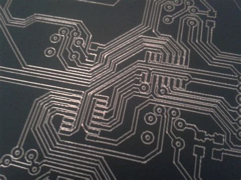
Laser cut printed circuit boards (PCBs) are an innovative way to rapidly prototype and manufacture electronic circuits. Using high-powered lasers, conductive traces and component footprints can be precisely cut into various substrate materials to create custom PCBs on-demand, without the need for traditional etching or milling processes.
Laser cutting technology offers several advantages over conventional PCB fabrication methods:
- Quick turnaround time – PCBs can be designed and cut within hours vs days or weeks
- Enables rapid prototyping and iteration of designs
- Compatible with a wide range of materials beyond standard FR4
- Allows creation of flexible and rigid-flex circuits
- Supports high-precision features and fine trace widths/spacing
- Environmentally friendly – no harsh chemicals required
In this comprehensive guide, we’ll dive into how laser cut PCBs are made, their benefits and limitations, common materials and specifications, design guidelines, and applications. By the end, you’ll have a solid understanding of this cutting-edge technology and how to leverage it for your own electronic projects.
How Laser Cut PCBs are Made
The laser cutting process for PCBs involves using a high-powered laser to selectively remove or ablate material from a substrate to create the desired circuit pattern. Let’s break down the key steps:
1. PCB Design
First, the PCB layout is designed using electronic design automation (EDA) software. The design includes the schematic, component placement, trace routing, and any other required features like mounting holes, cut-outs, etc.
2. Material Selection
Next, an appropriate substrate material is selected based on the project requirements. This could be a conventional copper-clad FR4 board, or alternative materials like aluminum, stainless steel, polyimide, or even paper for ultra-low cost applications.
3. Laser Cutting
The PCB design file is loaded into the laser cutter’s software, which controls the laser’s movement. A high-powered fiber or CO2 laser is focused onto the substrate surface. The laser beam ablates the material, vaporizing it to create the circuit pattern. The laser parameters (power, speed, frequency) are carefully tuned for the specific material and desired feature sizes.
4. Cleaning
After laser cutting, the PCB is cleaned to remove any debris or residue. Depending on the material, this may involve wiping with isopropyl alcohol, ultrasonic cleaning, or rinsing with water.
5. Surface Finish (Optional)
For improved durability or aesthetics, the PCB may be plated or coated with a surface finish like ENIG (immersion gold), OSP (organic solderability preservative), or HASL (hot air solder leveling).
6. Component Assembly
Finally, electronic components are soldered onto the PCB by hand or using automated pick-and-place equipment, completing the circuit board.

Laser Cut PCB Materials and Specifications
One of the key benefits of laser cutting is its compatibility with a diverse range of materials beyond traditional PCB substrates. Here are some of the most common options:
| Material | Composition | Thickness | Applications |
|---|---|---|---|
| FR4 | Glass-reinforced epoxy laminate | 0.4-3.2mm | General purpose, high-speed digital |
| Polyimide | Flexible polymer film | 0.05-0.5mm | Flexible circuits, wearables |
| Aluminum | Metal PCB | 0.4-3.2mm | High-power LEDs, heatsinking |
| Stainless Steel | Metal PCB | 0.2-1.0mm | Extreme environments, sensors |
| Paper | Cellulose-based | 0.15-0.3mm | Ultra-low cost, disposable |
Beyond material choice, laser cut PCBs can achieve very high precision in terms of minimum feature sizes:
| Specification | Typical Value |
|---|---|
| Minimum Trace/Space | 4 mil (0.1mm) |
| Minimum Hole Size | 8 mil (0.2mm) |
| Minimum Outline | 2 mil (0.05mm) |
| Layer Count | 1-4 |
| Copper Weight | 0.5-2.0 oz |
These specifications enable the creation of high-density PCB layouts with fine-pitch components. However, the achievable feature sizes and yield are ultimately dependent on the specific material, thickness, and laser parameters used.

Laser Cut PCB Design Guidelines
To ensure the best results when designing laser cut PCBs, follow these guidelines:
1. Trace Width and Spacing
Use wider traces where possible for improved current carrying capacity and manufacturing yield. Avoid using the minimum trace width for long runs or high-current paths. Maintain adequate spacing between traces to prevent short circuits.
2. Pad and Via Size
Pad and via sizes should be larger than the minimum hole size to allow for registration tolerances. For example, use a 20 mil pad for a 10 mil hole.
3. Copper Pour
Avoid large copper pours or planes, as they can degrade cut quality and increase manufacturing time. If a ground plane is needed, use a hatched or crosshatched pattern instead of solid copper.
4. Panelization
If cutting multiple PCBs, panelize them with adequate spacing between boards and use mouse bites or v-cuts for easy depaneling. Include fiducial markers to aid registration and assembly.
5. Solder Mask and Silkscreen
Solder mask and silkscreen layers can be challenging to achieve with laser cutting. If required, use a liquid photoimageable solder mask after cutting or consider alternate methods like vinyl stickers for component legends.
6. Design Rule Check (DRC)
Use EDA software to perform a design rule check before sending files for manufacturing. This helps catch any potential errors or manufacturability issues early in the design process.

Applications of Laser Cut PCBs
Laser cut PCBs are well-suited for a variety of applications across industries:
Prototyping and Product Development
The speed and flexibility of laser cutting makes it ideal for prototyping and iterating PCB designs. Engineers can quickly test and validate circuit functionality, component placement, and mechanical fit.
Flexible and Wearable Electronics
Laser cutting can create flexible circuits on thin polyimide films or textiles, enabling wearable devices, sensors, and smart clothing. The process supports fine features and can be used to create stretchable interconnects.
Internet of Things (IoT) Devices
Laser cut PCBs are a cost-effective option for IoT devices that may require custom shapes, cut-outs, or unconventional materials. The process is well-suited for low to medium volume production.
Education and Maker Projects
The accessibility and rapid turnaround of laser cutting make it popular for educational settings and maker projects. Students can design and manufacture their own PCBs, while hobbyists can create custom circuits for art, music, or home automation.
Research and Academia
Laser cut PCBs are used in research labs for prototyping novel sensors, microfluidics, and lab-on-a-chip devices. The process enables quick fabrication of custom geometries and integration of non-standard materials.
Frequently Asked Questions (FAQ)
1. What is the cost of laser cut PCBs compared to traditional manufacturing?
Laser cut PCBs are typically more expensive per unit than traditional PCBs for high volumes. However, for low quantities or quick-turn prototyping, laser cutting can be more cost-effective due to lower setup costs and faster turnaround times. The specific cost depends on the design complexity, material, and quantity.
2. How long does it take to manufacture a laser cut PCB?
The laser cutting process itself is relatively quick, often taking less than an hour for a small batch of PCBs. The total lead time, including design, material preparation, and shipping, is typically a few days to a week, depending on the supplier and your location. This is significantly faster than the multiple weeks required for traditional PCB manufacturing.
3. Can laser cut PCBs be used for high-frequency or RF applications?
Yes, laser cut PCBs can be used for high-frequency and RF applications, but with some limitations. The choice of substrate material is critical, as it affects the dielectric constant and loss tangent. Polyimide and PTFE-based materials are popular for these applications. However, laser cutting may introduce some surface roughness or irregularities that can impact signal integrity at very high frequencies. Careful design and material selection can help mitigate these issues.
4. Are laser cut PCBs durable and reliable?
Laser cut PCBs can be very durable and reliable, depending on the material and application. Polyimide and metal substrates offer excellent thermal stability, chemical resistance, and mechanical strength. However, the laser cutting process can create some localized heat-affected zones or micro-cracks that may impact long-term reliability in harsh environments. Proper material selection, post-processing, and quality control can help ensure the reliability of laser cut PCBs.
5. How do I choose a laser cutting service for my PCB project?
When selecting a laser cutting service for your PCB project, consider the following factors:
- Material availability: Ensure the service offers the substrates you require
- Cutting capabilities: Check the minimum feature sizes and tolerances achievable
- Turnaround time: Look for services with fast turnaround times to fit your schedule
- Pricing: Get quotes from multiple services and compare cost vs. performance
- Quality control: Ask about their quality control processes and inspections
- Customer support: Choose a service with responsive and knowledgeable support staff
It’s also helpful to read reviews and case studies from previous customers to gauge their experience and satisfaction with the service.
Conclusion
Laser cut PCBs offer a compelling alternative to traditional manufacturing methods, enabling rapid prototyping, flexible substrates, and high-precision features. By leveraging the speed and versatility of laser cutting, designers can bring their electronic creations to life faster and more cost-effectively than ever before.
As laser cutting technology continues to advance, we can expect to see even finer feature sizes, faster throughput, and compatibility with an ever-expanding range of materials. This will open up new possibilities for electronics applications in fields like wearables, IoT, and beyond.
To make the most of laser cut PCBs, it’s essential to understand the design guidelines, material properties, and manufacturing process. By following best practices and partnering with experienced laser cutting services, you can unlock the full potential of this exciting technology for your projects.
So whether you’re a seasoned engineer, student, or hobbyist, consider giving laser cut PCBs a try for your next electronic endeavor. With the power of lasers at your fingertips, the possibilities are truly endless!


Leave a Reply