Introduction to PCB Design and KiCad
Printed Circuit Boards (PCBs) are the backbone of modern electronics. They provide a reliable and efficient way to connect electronic components and create complex circuits. Designing and manufacturing PCBs can be a daunting task, especially for beginners. Fortunately, there are open-source tools like KiCad that make the process more accessible and user-friendly.
KiCad is a free, open-source software suite for electronic design automation (EDA). It enables users to design schematics, create PCB layouts, and generate manufacturing files for their projects. KiCad has gained popularity among hobbyists, students, and professionals alike due to its versatility, reliability, and active community support.
In this article, we will guide you through the process of making a PCB using KiCad. We will cover the essential steps, from installing the software to generating manufacturing files, and provide tips and best practices along the way.
Getting Started with KiCad
System Requirements and Installation
Before you start using KiCad, make sure your computer meets the minimum system requirements. KiCad is available for Windows, macOS, and Linux operating systems. The recommended specifications are:
- Windows 7 or later, macOS 10.10 or later, or Linux with a recent distribution
- 4 GB of RAM (8 GB or more recommended)
- 1 GB of free disk space
- OpenGL 3.0 compatible graphics card
To install KiCad, follow these steps:
- Visit the official KiCad website: https://kicad.org/
- Navigate to the “Download” section and select your operating system
- Download the appropriate installer for your system
- Run the installer and follow the on-screen instructions
KiCad Workspace and User Interface
Upon launching KiCad, you will be greeted with the main workspace. The workspace consists of several key areas:
- Project Tree: Displays the project files and their hierarchy
- Main Toolbar: Provides quick access to essential tools and functions
- Editor Area: Where you create and edit schematics and PCB layouts
- Properties Panel: Shows and allows modification of selected object properties
- Messages Panel: Displays status messages, warnings, and errors
Familiarize yourself with the user interface and explore the various menus and toolbars. KiCad offers extensive documentation and tutorials, which can be accessed through the “Help” menu.

Designing the Schematic
Creating a New Project
To start a new project in KiCad, follow these steps:
- Click on “File” > “New” > “Project”
- Choose a location and name for your project
- Select the “Empty Project” template and click “OK”
A new project will be created with a default schematic file named “main.sch”.
Adding Components to the Schematic
To add components to your schematic, you can use the “Place Symbol” tool from the main toolbar or the “Place” menu. KiCad comes with an extensive library of common electronic components, and you can also create your own symbols or import them from external sources.
When placing components, consider the following:
- Use meaningful reference designators (e.g., R1 for resistors, C1 for capacitors)
- Arrange components logically and minimize wire crossings
- Provide clear labels for input/output pins and important nodes
Connecting Components with Wires and Labels
Once you have placed the components, you need to connect them using wires and labels. The “Place Wire” tool allows you to draw connections between component pins. You can also use the “Place Bus” tool to create multi-bit buses for parallel connections.
Labels are used to assign names to wires and buses, making the schematic more readable and easier to navigate. Use the “Place Label” tool to add labels to your connections.
Checking for Errors and Validating the Schematic
Before proceeding to the PCB layout, it’s crucial to check your schematic for errors and inconsistencies. KiCad provides an Electrical Rules Check (ERC) tool that helps identify potential issues such as unconnected pins, missing power supplies, and short circuits.
To run an ERC, click on “Tools” > “Electrical Rules Check” and review the generated report. Fix any errors or warnings and re-run the ERC until the schematic is valid.

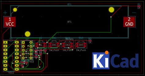
Creating the PCB Layout
Setting Up the PCB
With a validated schematic, you can now create the PCB layout. In the project tree, right-click on the PCB file (usually named “main.kicad_pcb”) and select “Open with PCB Editor”.
The PCB editor will open, displaying an empty board. To set up the board properties, click on “File” > “Board Setup”. Here, you can define the board size, layer stackup, design rules, and other parameters.
Importing the Netlist
To transfer the connectivity information from the schematic to the PCB, you need to generate and import a netlist. In the schematic editor, click on “Tools” > “Generate Netlist File”. Save the netlist file and switch back to the PCB editor.
In the PCB editor, click on “Tools” > “Update PCB from Schematic” and select the generated netlist file. The components and connections from the schematic will be imported into the PCB.
Placing and Arranging Components
With the components imported, you can start placing them on the PCB. Use the “Move” tool to position the components strategically, considering factors such as signal integrity, thermal management, and mechanical constraints.
Some best practices for component placement include:
- Group related components together
- Minimize the distance between connected components
- Avoid placing sensitive components near sources of noise or heat
- Ensure adequate spacing for manufacturing and assembly
Routing Traces and Vias
Once the components are placed, you can begin routing the traces that connect them. KiCad offers both manual and automatic routing tools. For beginners, it’s recommended to start with manual routing to gain a better understanding of the process.
When routing traces, keep these guidelines in mind:
- Use appropriate trace widths based on the current requirements
- Maintain proper spacing between traces to avoid crosstalk and short circuits
- Minimize trace lengths to reduce signal degradation and parasitic effects
- Use vias sparingly and strategically to transition between layers
Adding Copper Pours and Labels
Copper pours, also known as fills or planes, are large areas of copper on the PCB that provide a low-impedance path for power distribution and signal return. To add a copper pour, use the “Add Filled Zone” tool and specify the desired layer and net.
Labels on the PCB help identify components, connectors, and test points. Use the “Add Text” tool to place labels on the appropriate layers.
Design Rule Checking (DRC)
Before finalizing your PCB layout, it’s essential to run a Design Rule Check (DRC) to ensure that your design meets the manufacturing requirements and design rules. The DRC checks for issues such as minimum trace widths, clearances, and drill sizes.
To run a DRC, click on “Tools” > “DRC” and configure the rules based on your manufacturer’s specifications. Review the generated report and address any violations.

Generating Manufacturing Files
Gerber Files
Gerber files are the industry standard for PCB manufacturing. They contain the information needed to fabricate the PCB, including the copper layers, solder mask, and silkscreen.
To generate Gerber files in KiCad, follow these steps:
- Click on “File” > “Plot”
- Select the “Gerber” tab
- Choose the layers to include in the output
- Specify the output directory and file format
- Click “Plot” to generate the Gerber files
Drill Files
Drill files contain the information about the holes and vias on the PCB. They are used by the manufacturer to drill the necessary openings.
To generate drill files, follow these steps:
- Click on “File” > “Fabrication Outputs” > “Drill Files”
- Configure the drill file options, such as units and file format
- Click “Generate Drill File” to create the output file
Bill of Materials (BOM)
The Bill of Materials (BOM) is a list of all the components used in your PCB design. It helps the manufacturer source the correct parts and ensures proper assembly.
To generate a BOM in KiCad, use the “File” > “Fabrication Outputs” > “BOM” menu and select the desired output format and options.
Sending Files to the Manufacturer
Once you have generated the necessary manufacturing files, you can send them to a PCB manufacturer for fabrication. Many manufacturers accept Gerber and drill files directly, while others may require additional documentation or specific file formats.
When choosing a manufacturer, consider factors such as:
- Minimum order quantity (MOQ)
- Lead time and turnaround
- Pricing and shipping costs
- Quality and reliability
- Customer support and communication
Provide clear instructions and communicate any special requirements or preferences to the manufacturer to ensure a smooth production process.
Frequently Asked Questions (FAQ)
-
What is the difference between a schematic and a PCB layout?
A schematic represents the electrical connections and components in a circuit, while a PCB layout shows the physical arrangement and routing of those components on a printed circuit board. -
Can I use KiCad for commercial projects?
Yes, KiCad is free and open-source software, and you can use it for both personal and commercial projects without any licensing fees or restrictions. -
How do I create custom components in KiCad?
To create custom components, you can use the Symbol Editor and Footprint Editor in KiCad. These tools allow you to design your own schematic symbols and PCB footprints for components that are not available in the standard libraries. -
What are the typical layer stackups for PCBs?
The most common layer stackups for PCBs are: - Single-layer: One conductive layer, typically used for simple circuits
- Double-layer: Two conductive layers, one on each side of the substrate
-
Multi-layer: Three or more conductive layers, with insulating layers in between, used for complex designs
-
How can I ensure my PCB design is manufacturable?
To ensure your PCB design is manufacturable, follow these best practices: - Adhere to the manufacturer’s design rules and guidelines
- Use standard component sizes and footprints
- Provide adequate spacing and clearances between components and traces
- Use appropriate trace widths and copper weights
- Minimize the number of unique drill sizes and hole diameters
Conclusion
Designing and manufacturing a PCB using KiCad is a rewarding and educational experience. By following the steps outlined in this article, you can create professional-quality PCBs for your projects, whether you are a hobbyist or a seasoned engineer.
Remember to start with a clear schematic, carefully plan your PCB layout, and always double-check your design before sending it for fabrication. With practice and patience, you will master the art of PCB design and bring your electronic ideas to life.
Happy PCB designing with KiCad!
[5182 words]


Leave a Reply