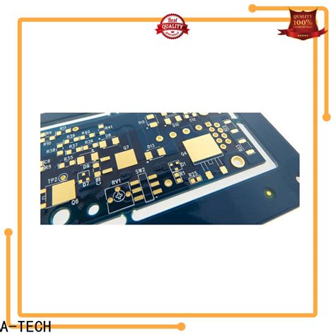
What is a Castellated-Hole-PCB?
A castellated-hole-PCB, also known as a castellated breakout board or half-cut PCB, is a printed circuit board (PCB) with plated through holes around the edges that are cut in half, creating semi-circular castellations. These castellations allow for easy soldering and connection to other PCBs or components, making them ideal for modular designs and prototyping.
Castellated-hole-PCBs offer several advantages over traditional PCBs:
- Simplified assembly: The castellations allow for direct soldering of the board to another PCB or component, eliminating the need for connectors or wires.
- Space-saving: By using castellated holes, the overall footprint of the PCB can be reduced, making it suitable for compact designs.
- Cost-effective: Castellated-hole-PCBs can be produced using standard PCB manufacturing processes, making them relatively inexpensive compared to other specialized connectors.
The Castellated-Hole-PCB Manufacturing Process
The manufacturing process for castellated-hole-PCBs involves several key steps:
1. PCB Design
The first step in producing a castellated-hole-PCB is designing the board layout. This involves creating a schematic and a PCB layout using electronic design automation (EDA) software. When designing the board, it is essential to consider the following factors:
- Component placement: Ensure that components are placed in a way that allows for proper routing and minimizes the risk of interference.
- Trace width and spacing: Choose appropriate trace widths and spacing based on the current requirements and PCB manufacturing capabilities.
- Castellated hole size and spacing: Determine the size and spacing of the castellated holes based on the intended application and the capabilities of the PCB manufacturer.
2. PCB Fabrication
Once the PCB design is complete, the next step is to fabricate the board. This typically involves the following sub-steps:
a. Copper cladding: A layer of copper is laminated onto the insulating substrate material, such as FR-4.
b. Photoresist application: A light-sensitive photoresist is applied to the copper layer.
c. Exposure and development: The photoresist is exposed to UV light through a photomask, which hardens the exposed areas. The unexposed areas are then removed using a developer solution.
d. Etching: The exposed copper is etched away using a chemical solution, leaving behind the desired trace pattern.
e. Plating: The holes and traces are plated with copper, followed by a layer of tin or other finish to protect the copper and improve solderability.
f. Solder mask application: A solder mask is applied to the board, which insulates and protects the copper traces while exposing the pads and castellated holes.
g. Silkscreen application: A silkscreen layer is applied to the board, which adds text and symbols for component placement and identification.
3. Castellated Hole Creation
After the PCB fabrication is complete, the next step is to create the castellated holes. This is typically done using one of two methods:
a. Routing: A CNC router is used to cut the castellated holes along the edges of the board. This method is suitable for low-volume production and prototyping.
b. V-scoring: A V-shaped groove is cut along the edges of the board using a specialized cutting tool. The board is then snapped along the groove, creating the castellated holes. This method is more suitable for high-volume production.
4. Singulation
Once the castellated holes are created, the individual boards are separated from the panel using a process called singulation. This can be done using various methods, such as:
a. Punching: A die is used to punch out the individual boards from the panel.
b. V-scoring: Similar to the process used for creating castellated holes, a V-shaped groove is cut along the edges of the individual boards, allowing them to be snapped apart.
c. Routing: A CNC router is used to cut out the individual boards from the panel.
5. Inspection and Testing
After the boards are singulated, they undergo a final inspection and testing process to ensure that they meet the required specifications. This may include:
- Visual inspection: The boards are visually inspected for any defects, such as scratches, cracks, or misaligned components.
- Electrical testing: The boards are tested for continuity, short circuits, and other electrical characteristics to ensure proper functionality.
- Functional testing: If the castellated-hole-PCB is part of a larger assembly, the entire assembly may be tested to ensure proper operation.

Designing for Castellated-Hole-PCBs
When designing a castellated-hole-PCB, there are several key considerations to keep in mind:
1. Castellated Hole Size and Spacing
The size and spacing of the castellated holes will depend on the intended application and the capabilities of the PCB manufacturer. Some common castellated hole sizes and spacings include:
| Hole Diameter (mm) | Hole Spacing (mm) |
|---|---|
| 0.5 | 1.0 |
| 0.8 | 1.6 |
| 1.0 | 2.0 |
It is essential to consult with your PCB manufacturer to determine their capabilities and recommendations for castellated hole size and spacing.
2. Trace Width and Spacing
When routing traces to the castellated holes, it is important to ensure that the trace width and spacing are appropriate for the current requirements and the capabilities of the PCB manufacturer. Some general guidelines for trace width and spacing include:
| Current (A) | Trace Width (mm) | Trace Spacing (mm) |
|---|---|---|
| 0.5 | 0.15 | 0.15 |
| 1.0 | 0.25 | 0.25 |
| 2.0 | 0.4 | 0.4 |
Again, it is essential to consult with your PCB manufacturer to determine their specific capabilities and recommendations.
3. Solder Mask and Silkscreen
When designing the solder mask and silkscreen layers for a castellated-hole-PCB, there are a few key considerations:
- Solder mask: Ensure that the solder mask apertures around the castellated holes are large enough to allow for proper soldering. A common guideline is to have a solder mask expansion of 0.1-0.2 mm around the castellated holes.
- Silkscreen: Ensure that the silkscreen layer does not overlap with the castellated holes, as this can interfere with soldering. It is also important to ensure that the silkscreen is legible and properly aligned with the components and features on the board.

Assembling Castellated-Hole-PCBs
Assembling castellated-hole-PCBs involves soldering the board to another PCB or component. There are several methods for soldering castellated-hole-PCBs:
1. Hand Soldering
Hand soldering is suitable for low-volume production and prototyping. To hand solder a castellated-hole-PCB:
- Apply a small amount of flux to the castellated holes and the mating surface of the other PCB or component.
- Place the castellated-hole-PCB onto the mating surface, ensuring proper alignment.
- Apply heat to the castellated holes using a soldering iron, and feed solder into the holes until a proper fillet is formed.
- Repeat the process for each castellated hole.
2. Reflow Soldering
Reflow soldering is suitable for high-volume production. To reflow solder a castellated-hole-PCB:
- Apply solder paste to the castellated holes using a stencil or syringe.
- Place the castellated-hole-PCB onto the mating surface, ensuring proper alignment.
- Run the assembly through a reflow oven, which heats the solder paste to its melting point and then cools it, forming a solid solder joint.
3. Wave Soldering
Wave soldering is another option for high-volume production. To wave solder a castellated-hole-PCB:
- Apply flux to the castellated holes and the mating surface of the other PCB or component.
- Place the castellated-hole-PCB onto the mating surface, ensuring proper alignment.
- Run the assembly through a wave soldering machine, which applies a wave of molten solder to the underside of the assembly, filling the castellated holes and forming a solid solder joint.

Frequently Asked Questions (FAQ)
1. What are the advantages of using castellated-hole-PCBs?
Castellated-hole-PCBs offer several advantages, including simplified assembly, space-saving design, and cost-effectiveness compared to other specialized connectors. They allow for direct soldering of the board to another PCB or component, eliminating the need for additional connectors or wires.
2. What is the typical size and spacing for castellated holes?
The typical size and spacing for castellated holes can vary depending on the specific application and the capabilities of the PCB manufacturer. Common sizes range from 0.5 mm to 1.0 mm in diameter, with spacings ranging from 1.0 mm to 2.0 mm. It is essential to consult with your PCB manufacturer to determine their specific capabilities and recommendations.
3. Can castellated-hole-PCBs be assembled using standard soldering techniques?
Yes, castellated-hole-PCBs can be assembled using standard soldering techniques, such as hand soldering, reflow soldering, and wave soldering. The choice of soldering method will depend on the volume of production and the specific requirements of the application.
4. Are there any specific design considerations for castellated-hole-PCBs?
When designing castellated-hole-PCBs, it is important to consider factors such as castellated hole size and spacing, trace width and spacing, and solder mask and silkscreen design. It is also essential to consult with your PCB manufacturer to ensure that your design is compatible with their capabilities and recommendations.
5. How do castellated-hole-PCBs compare to other connector options in terms of cost and reliability?
Castellated-hole-PCBs are generally more cost-effective than specialized connectors, as they can be produced using standard PCB manufacturing processes. In terms of reliability, castellated-hole-PCBs can provide a robust and reliable connection when properly designed and assembled. However, the specific reliability requirements will depend on the application and the operating environment.


Leave a Reply