Understanding the Basics of PCB Manufacturing
Before we dive into the manufacturing process, let’s establish a foundational understanding of PCBs. A PCB is a flat board made of insulating materials, such as fiberglass or composite epoxy, with conductive copper traces etched onto its surface. These traces form the electrical connections between components, allowing for the flow of signals and power throughout the circuit.
PCBs come in various types, depending on the number of layers and the specific manufacturing techniques employed. The most common types include:
- Single-sided PCBs: These have copper traces on only one side of the board.
- Double-sided PCBs: These have copper traces on both sides of the board, with through-hole connections linking the two sides.
- Multi-layer PCBs: These consist of multiple layers of insulating material and copper traces, allowing for more complex routing and higher component density.
Key Terminology in PCB Manufacturing
To better understand the PCB manufacturing process, familiarize yourself with the following key terms:
- Substrate: The insulating material that forms the base of the PCB.
- Copper Foil: The thin layer of copper that is laminated onto the substrate.
- Solder Mask: A protective coating applied to the PCB to prevent accidental short circuits and provide insulation.
- Silkscreen: The text and symbols printed on the PCB for component identification and assembly guidance.
- Drilling: The process of creating holes in the PCB for through-hole components and vias.
- Etching: The process of removing unwanted copper from the PCB to create the desired circuit pattern.
- Plating: The process of applying additional copper or other metals to the PCB to improve conductivity and protect against corrosion.
The PCB Manufacturing Process: Step by Step
The PCB manufacturing process consists of several key stages, each contributing to the creation of a high-quality and functional board. Let’s explore these stages in detail.
Step 1: PCB Design and Prototyping
The PCB manufacturing process begins with the design phase. Engineers use specialized software to create a schematic diagram of the circuit, specifying the components and their interconnections. This schematic is then translated into a physical layout, determining the placement of components and the routing of traces on the board.
Once the design is finalized, a prototype PCB is often created to validate the functionality and identify any potential issues. Prototyping allows for iterative refinements to the design before proceeding to mass production.
Step 2: PCB Fabrication
With the design finalized, the next stage is PCB fabrication. This involves several sub-steps:
-
Substrate Preparation: The substrate material is cut to the desired size and shape. Copper foil is then laminated onto the substrate using heat and pressure.
-
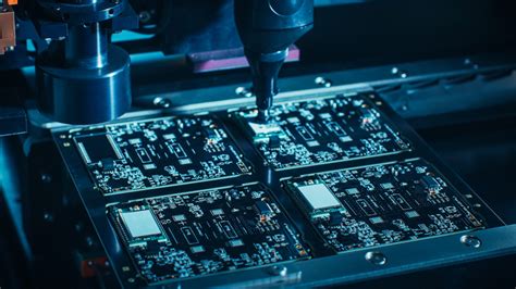
Drilling: Holes are drilled into the PCB at precise locations to accommodate through-hole components and create vias for inter-layer connections. Modern PCB manufacturing often employs computer-controlled drilling machines for high accuracy.
-
Copper Patterning: The desired circuit pattern is transferred onto the copper layer through a process called photolithography. This involves applying a light-sensitive photoresist coating to the copper, exposing it to UV light through a patterned mask, and then developing the photoresist to reveal the desired copper traces.
-
Etching: The exposed copper is chemically etched away, leaving only the desired circuit pattern on the substrate. The remaining photoresist is then stripped off.
-
Plating: Additional copper or other metals, such as gold or silver, may be plated onto the PCB to improve conductivity, protect against corrosion, or facilitate soldering.
-
Solder Mask Application: A solder mask is applied to the PCB, covering the copper traces while leaving the component pads exposed. This protects against accidental short circuits and provides insulation.
-
Silkscreen Printing: Text, symbols, and other markings are printed onto the PCB using a silkscreen process. This aids in component identification and assembly.
Step 3: PCB Assembly
Once the bare PCB is fabricated, it moves on to the assembly stage, where electronic components are mounted onto the board. This stage involves several sub-steps:
-
Solder Paste Application: Solder paste, a mixture of tiny solder particles suspended in a flux medium, is applied to the component pads on the PCB using a stencil or screen printing process.
-
Component Placement: Electronic components, such as resistors, capacitors, and integrated circuits, are placed onto the solder paste-coated pads. This is typically done using automated pick-and-place machines for high-volume production, while smaller batches may involve manual placement.
-
Reflow Soldering: The PCB with the placed components is passed through a reflow oven, which applies a controlled heat profile to melt the solder paste and form a permanent bond between the components and the PCB.
-
Through-Hole Component Insertion: If the PCB design includes through-hole components, they are manually inserted into the corresponding holes and soldered in place using a wave soldering machine or hand soldering techniques.
-
Inspection and Testing: The assembled PCB undergoes visual inspection and automated optical inspection (AOI) to identify any defects or misaligned components. Electrical testing is also performed to ensure proper functionality and adherence to specifications.
Step 4: PCB Finishing and Packaging
After assembly, the PCB undergoes final finishing and packaging steps:
-
Conformal Coating: If required, a protective coating is applied to the PCB to shield it from environmental factors such as moisture, dust, and contaminants.
-
Labeling: Unique identifiers, such as serial numbers or barcodes, are labeled onto the PCB for traceability and inventory management.
-
Packaging: The finished PCBs are packaged according to customer requirements, which may include individual bagging, bulk packaging, or custom packaging solutions.

Quality Control in PCB Manufacturing
Ensuring the quality and reliability of PCBs is crucial in the manufacturing process. Several quality control measures are implemented at various stages:
-
Design Rule Checks (DRC): DRC is performed during the design phase to verify that the PCB layout adheres to the manufacturing guidelines and constraints, such as minimum trace widths, clearances, and drill sizes.
-
Automated Optical Inspection (AOI): AOI systems use high-resolution cameras and advanced image processing algorithms to inspect the PCB for defects, such as missing components, solder bridges, or incorrect component placement.
-
Electrical Testing: Functional testing is conducted to verify the electrical performance of the PCB, including continuity, insulation resistance, and signal integrity.
-
Environmental Testing: PCBs may undergo environmental testing, such as thermal cycling or humidity exposure, to ensure their reliability under various operating conditions.
-
Statistical Process Control (SPC): SPC techniques are employed to monitor and control the manufacturing process, identifying trends and variations that may impact product quality.

Advancements in PCB Manufacturing Technology
The PCB manufacturing industry continues to evolve, driven by the demand for miniaturization, higher performance, and increased functionality. Some notable advancements include:
-
High-Density Interconnect (HDI) PCBs: HDI technology allows for finer trace widths, smaller vias, and higher component density, enabling the creation of more compact and complex PCBs.
-
Embedded Components: Components such as capacitors and resistors can be embedded within the PCB substrate, saving space and improving electrical performance.
-
Flexible and Rigid-Flex PCBs: Flexible PCBs and rigid-flex combinations offer increased design flexibility, allowing for the creation of three-dimensional and space-saving configurations.
-
3D Printing: Additive manufacturing techniques, such as 3D printing, are being explored for PCB fabrication, potentially offering faster prototyping and customization options.

Frequently Asked Questions (FAQ)
-
What is the typical turnaround time for PCB manufacturing?
The turnaround time for PCB manufacturing varies depending on the complexity of the design, the volume of the order, and the specific manufacturing processes required. For standard PCBs, the typical turnaround time ranges from a few days to a couple of weeks. Rush services may be available for faster delivery, but they often come at a higher cost. -
Can I manufacture PCBs with multiple layers?
Yes, PCBs can be manufactured with multiple layers. Multi-layer PCBs are commonly used for complex designs that require a higher component density and more intricate routing. The number of layers can range from four to over thirty, depending on the specific requirements of the application. -
What materials are used for PCB substrates?
The most common materials used for PCB substrates are: - FR-4: A flame-retardant fiberglass-reinforced epoxy laminate, widely used for general-purpose PCBs.
- Polyimide: A high-temperature and flexible substrate material, often used for flexible PCBs and applications requiring thermal stability.
- Ceramic: Used for high-frequency and high-temperature applications, offering excellent electrical insulation and thermal conductivity.
-
Metal Core: PCBs with a metal substrate, such as aluminum, are used for applications requiring efficient heat dissipation.
-
What are the different surface finishes available for PCBs?
Some common surface finishes for PCBs include: - Hot Air Solder Leveling (HASL): A tin-lead alloy is applied to the PCB pads and then leveled using hot air, providing a solderable surface.
- Electroless Nickel Immersion Gold (ENIG): A layer of nickel is plated onto the copper pads, followed by a thin layer of gold, offering excellent solderability and shelf life.
- Immersion Silver: A thin layer of silver is chemically deposited onto the copper pads, providing good solderability and cost-effectiveness.
-
Organic Solderability Preservative (OSP): A thin, organic coating is applied to the copper pads to prevent oxidation and ensure solderability.
-
How do I ensure the manufacturability of my PCB design?
To ensure the manufacturability of your PCB design, consider the following guidelines: - Adhere to the design rules and constraints provided by your PCB manufacturer, including minimum trace widths, clearances, and drill sizes.
- Use standard component packages and footprints whenever possible to avoid custom manufacturing requirements.
- Provide clear and accurate documentation, including bill of materials (BOM), assembly drawings, and Gerber files.
- Conduct design rule checks (DRC) and manufacturability checks using your PCB design software to identify and resolve any potential issues.
- Communicate with your PCB manufacturer early in the design process to discuss any specific requirements or constraints.
Conclusion
The PCB manufacturing process is a complex and precise sequence of steps that transforms a design concept into a functional printed circuit board. From design and prototyping to fabrication, assembly, and finishing, each stage plays a crucial role in ensuring the quality and reliability of the final product.
As technology continues to advance, PCB manufacturing evolves to meet the ever-increasing demands for miniaturization, higher performance, and increased functionality. By understanding the intricacies of the manufacturing process and staying updated with the latest advancements, designers and engineers can create PCBs that push the boundaries of electronic innovation.
Whether you are a seasoned engineer or a curious learner, delving into the world of PCB manufacturing provides valuable insights into the backbone of modern electronics. By mastering the art and science of PCB manufacturing, you can bring your electronic visions to life and contribute to the ever-expanding landscape of technological progress.
| PCB Manufacturing Process | Key Steps |
|---|---|
| Design and Prototyping | Schematic design, layout, prototyping |
| Fabrication | Substrate preparation, drilling, copper patterning, etching, plating, solder mask application, silkscreen printing |
| Assembly | Solder paste application, component placement, reflow soldering, through-hole component insertion, inspection and testing |
| Finishing and Packaging | Conformal coating, labeling, packaging |
Word count: 2070 words


Leave a Reply