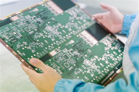
What is Multilayer PCB Pressing?
Multilayer PCB pressing is a crucial step in the manufacturing process of printed circuit boards (PCBs) with more than two layers. It involves the lamination of multiple layers of Copper Foil, prepreg (pre-impregnated fiberglass), and core materials under high pressure and temperature to create a single, solid board. This process ensures proper bonding between layers, maintains the desired thickness, and helps achieve the required mechanical and electrical properties of the final PCB.
Benefits of Multilayer PCB Pressing
- Increased circuit density: Multilayer PCBs allow for more complex designs and higher component density compared to single or double-layer boards.
- Improved signal integrity: Proper pressing minimizes signal interference and crosstalk between layers, ensuring better signal integrity.
- Enhanced mechanical strength: The lamination process creates a strong, durable board that can withstand various environmental factors and mechanical stresses.
- Reduced board size: By utilizing multiple layers, designers can minimize the overall size of the PCB while maintaining the required functionality.
Multilayer PCB Pressing Process
1. Material Preparation
Before pressing, the necessary materials must be prepared:
- Copper foil: The conductive layers of the PCB, typically ranging from 0.5 oz to 2 oz in thickness.
- Prepreg: A partially cured fiberglass material pre-impregnated with epoxy resin, acting as an insulating layer between copper foils.
- Core materials: Fully cured Fiberglass Laminates used as the base for the inner layers of the PCB.
Common Prepreg and Core Material Thicknesses
| Material | Thickness (mm) |
|---|---|
| Prepreg | 0.05 – 0.30 |
| Core | 0.20 – 1.60 |
2. Layer Stacking
The prepared materials are stacked in a specific order, alternating between copper foil, prepreg, and core layers. The stacking order depends on the desired number of layers and the PCB design requirements.
Example 4-layer PCB stacking order:
1. Copper foil (top layer)
2. Prepreg
3. Core (inner layer 1)
4. Prepreg
5. Core (inner layer 2)
6. Prepreg
7. Copper foil (bottom layer)
3. Lamination
The stacked layers are placed in a special press that applies high pressure and heat to the assembly. The lamination process typically involves two stages:
- Vacuum lamination: The stacked layers are placed in a vacuum bag to remove any air between the layers, ensuring proper contact and preventing voids.
- Hot pressing: The vacuum-sealed stack is placed in a heated press, where it is subjected to high pressure (200-400 psi) and temperature (180-200°C) for a specific duration (1-2 hours).
Typical Lamination Parameters
| Parameter | Value Range |
|---|---|
| Pressure | 200 – 400 psi |
| Temperature | 180 – 200°C |
| Duration | 1 – 2 hours |
The heat and pressure cause the prepreg to melt and flow, bonding the layers together and creating a solid, uniform board.
4. Cooling and Inspection
After lamination, the PCB is cooled gradually to room temperature to prevent warping or delamination. The pressed board is then inspected for any defects, such as voids, delamination, or uneven thickness. If the board passes inspection, it proceeds to the next stages of the PCB manufacturing process, such as drilling, plating, and solder mask application.

Factors Affecting Multilayer PCB Pressing Quality
Several factors can influence the quality of the pressed multilayer PCB:
- Material selection: Choosing compatible and high-quality copper foil, prepreg, and core materials is essential for achieving optimal results.
- Stacking accuracy: Precise alignment of the layers during stacking is crucial to ensure proper registration of the circuitry across the layers.
- Lamination parameters: Pressure, temperature, and duration must be carefully controlled to achieve proper bonding without damaging the materials or components.
- Cleanliness: Contamination between layers can lead to voids, delamination, or poor bonding. Maintaining a clean environment and handling materials properly is essential.
- Copper foil thickness: The thickness of the copper foil can affect the pressing process, as thinner foils may require different lamination parameters compared to thicker ones.

Troubleshooting Common Multilayer PCB Pressing Issues
1. Voids
Voids are air pockets that form between layers during the pressing process. They can weaken the board’s mechanical strength and cause electrical issues. Possible causes and solutions include:
- Insufficient vacuum during lamination: Ensure proper vacuum sealing of the stack before pressing.
- Contamination between layers: Maintain cleanliness during material handling and stacking.
- Incompatible materials: Use materials with matched thermal expansion coefficients and compatible resin systems.
2. Delamination
Delamination refers to the separation of layers within the PCB, which can lead to mechanical and electrical failures. Possible causes and solutions include:
- Improper lamination parameters: Optimize pressure, temperature, and duration settings for the specific materials used.
- Uneven pressure distribution: Ensure the press applies uniform pressure across the entire board surface.
- Rapid cooling after lamination: Allow the board to cool gradually to room temperature to minimize stress.
3. Warping
Warping is the distortion of the PCB’s shape, which can cause issues during subsequent manufacturing processes and affect the final assembly. Possible causes and solutions include:
- Unbalanced Copper Distribution: Balance the copper coverage across layers to minimize stress differences.
- Excessive lamination temperature: Adjust the temperature to the optimal range for the materials used.
- Improper cooling: Implement a controlled cooling process to reduce thermal stress on the board.

FAQ
- What is the difference between prepreg and core materials in Multilayer PCBs?
-
Prepreg is a partially cured fiberglass material pre-impregnated with epoxy resin, used as an insulating layer between copper foils. Core materials are fully cured fiberglass laminates that serve as the base for the inner layers of the PCB.
-
How does the number of layers affect the pressing process?
-
As the number of layers increases, the stacking order becomes more complex, and the lamination parameters (pressure, temperature, and duration) may need to be adjusted to ensure proper bonding between all layers.
-
Can multilayer PCBs be pressed using different materials for each layer?
-
Yes, it is possible to use different materials for each layer, such as varying the prepreg thickness or using different core materials. However, the materials must be compatible and have similar thermal expansion coefficients to prevent issues like delamination or warping.
-
What is the purpose of vacuum lamination in the pressing process?
-
Vacuum lamination is used to remove any air between the layers of the PCB stack before hot pressing. This ensures proper contact between the layers and prevents the formation of voids, which can weaken the board’s mechanical strength and cause electrical issues.
-
How can I prevent warping in multilayer PCBs during the pressing process?
- To prevent warping, ensure a balanced copper distribution across layers, use optimal lamination parameters (pressure, temperature, and duration) for the materials used, and implement a controlled cooling process after lamination to minimize thermal stress on the board.
Conclusion
Multilayer PCB pressing is a critical step in the manufacturing process of complex, high-density printed circuit boards. By understanding the materials, stacking order, lamination process, and factors affecting pressing quality, manufacturers can produce reliable and robust multilayer PCBs. Proper control of the pressing process parameters, material selection, and handling can help prevent common issues such as voids, delamination, and warping, ensuring the final PCB meets the desired mechanical and electrical requirements.


Leave a Reply