Introduction to PCBs and Fritzing
Printed circuit boards, or PCBs, are the foundation of nearly all modern electronics. These boards mechanically support and electrically connect electronic components using conductive pathways, tracks or signal traces etched from copper sheets laminated onto a non-conductive substrate.
Designing custom PCBs used to require specialized knowledge and expensive software. But now, open source programs like Fritzing make PCB design accessible to makers, hobbyists, students and engineers of all skill levels.
What is Fritzing?
Fritzing is a free, open-source hardware initiative that makes electronics accessible as a creative material for anyone. It offers a software tool, a community website and services in the spirit of Processing and Arduino, fostering a creative ecosystem that allows users to document their prototypes, share them with others, teach electronics in a classroom, and lay out and manufacture professional PCBs.
The Fritzing application is an Electronic Design Automation (EDA) tool aimed at supporting designers, artists, researchers and hobbyists to take the step from physical prototyping to actual product. It allows users to create schematics by selecting parts from a large part library, connect them with wires, and lay them out on a virtual breadboard. The resulting sketch can then be used as a basis to design PCBs that can be easily fabricated.
Why Use Fritzing for PCB Design?
There are many reasons why Fritzing is a great choice for PCB design, especially for beginners and hobbyists:
- Ease of use: Fritzing has a simple, intuitive interface that makes it easy to design circuits and PCBs without extensive knowledge or experience.
- Large part library: Fritzing comes with a large library of components that you can use in your designs, from basic parts like resistors and capacitors to more complex modules like Arduino boards and sensors.
- Breadboard view: Fritzing allows you to design circuits on a virtual breadboard, which makes it easy to prototype and test your designs before committing to a PCB.
- Schematic view: Once you’ve designed your circuit on the breadboard, you can switch to the schematic view to create a more formal diagram of your circuit.
- PCB view: Finally, you can switch to the PCB view to lay out your components and traces on a virtual PCB. Fritzing will automatically route the traces based on your schematic, but you can also manually adjust them as needed.
- Fabrication support: Once your PCB design is complete, you can generate Gerber files and send them to a fabrication service to have your boards manufactured.
Getting Started with Fritzing
To get started with Fritzing, you’ll need to download and install the software on your computer. Fritzing is available for Windows, Mac, and Linux, and you can download the latest version from the official website: https://fritzing.org/download/
Once you’ve installed Fritzing, you can launch the application and start designing your first PCB.
The Fritzing Interface
The Fritzing interface is divided into three main views:
- Breadboard view: This is where you can design your circuit on a virtual breadboard, just like you would with a physical breadboard. You can add components from the parts library and connect them with wires.
- Schematic view: This is a more formal representation of your circuit, using standard schematic symbols for components and nets for connections.
- PCB view: This is where you can lay out your components and traces on a virtual PCB. Fritzing will automatically generate a PCB layout based on your schematic, but you can also manually adjust it as needed.
You can switch between these views using the tabs at the top of the window.
The Parts Library
One of the key features of Fritzing is its extensive parts library, which includes a wide range of components that you can use in your designs. To access the parts library, click the “Core Parts” button in the toolbar or go to Window > Parts.
The parts library is organized into categories, such as “Basic Parts”, “Input Devices”, “Output Devices”, “Arduino”, and more. You can browse the categories to find the part you need, or use the search bar to search for a specific part by name or description.
To add a part to your design, simply drag it from the parts library onto the breadboard view. You can then use the part in your circuit by connecting it to other components with wires.

Designing a Simple Circuit in Fritzing
Let’s walk through the process of designing a simple LED circuit in Fritzing. This circuit will consist of an LED, a resistor, and a power source (in this case, a battery).
Step 1: Add Components to the Breadboard
Start by adding the following components to the breadboard view:
- LED (any color)
- 330 ohm resistor
- Battery (9V)
You can find these components in the “Core Parts” library under the “Basic” and “Power” categories.
Step 2: Connect the Components
Next, connect the components with wires to create the following circuit:
- Connect the positive lead of the battery to one end of the resistor.
- Connect the other end of the resistor to the anode (longer leg) of the LED.
- Connect the cathode (shorter leg) of the LED to the negative lead of the battery.
Your breadboard view should look something like this:
| Component | Connection |
|---|---|
| Battery (+) | Resistor |
| Resistor | LED (anode) |
| LED (cathode) | Battery (-) |
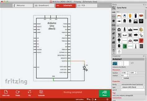
Step 3: Switch to Schematic View
Now that you’ve designed your circuit on the breadboard, switch to the schematic view by clicking the “Schematic” tab at the top of the window.
Fritzing will automatically generate a schematic diagram based on your breadboard design. You may need to rearrange the components and nets to make the schematic more readable.
Step 4: Switch to PCB View
Finally, switch to the PCB view by clicking the “PCB” tab at the top of the window.
Fritzing will automatically generate a PCB layout based on your schematic. The components will be placed on the board and the traces will be routed automatically.
You can manually adjust the placement of components and routing of traces as needed. You can also adjust the size and shape of the PCB by clicking and dragging the edges of the board.
Step 5: Export Gerber Files
Once you’re happy with your PCB layout, you can generate Gerber files to send to a fabrication service. To do this, go to File > Export > for Production > Extended Gerber (RS-274X).
Fritzing will generate a zip file containing the Gerber files for your PCB. You can send this file to a fabrication service to have your boards manufactured.

Advanced PCB Design Techniques
While the basics of PCB design in Fritzing are relatively simple, there are many advanced techniques that you can use to create more complex and professional-looking boards. Here are a few tips and tricks to keep in mind:
Use Ground Planes
A ground plane is a large area of copper on the PCB that is connected to ground. Using a ground plane can help reduce electromagnetic interference (EMI) and improve the overall performance of your circuit.
To create a ground plane in Fritzing, simply create a large rectangular trace and connect it to the ground net. You can then route other traces around the ground plane as needed.
Use Vias
Vias are small holes drilled through the PCB that allow you to connect traces on different layers of the board. Using vias can help you route traces more efficiently and reduce the overall size of your board.
To create a via in Fritzing, simply place a via component on the board and connect it to the appropriate traces. You can adjust the size and shape of the via as needed.
Use Custom Footprints
Fritzing comes with a large library of component footprints, but sometimes you may need to create your own custom footprint for a specific component. To do this, you can use the “Part Editor” tool in Fritzing.
To access the Part Editor, go to Window > Part Editor. From here, you can create a new footprint by drawing shapes and pads on the canvas. You can then save your custom footprint and use it in your designs.
Use Copper Pours
Copper pours are large areas of copper on the PCB that are not connected to any particular net. Using copper pours can help improve the mechanical strength of the board and provide additional shielding against EMI.
To create a copper pour in Fritzing, simply create a large rectangular trace and set its net to “None”. You can then place the copper pour on the board and route other traces around it as needed.

Common Pitfalls and How to Avoid Them
While PCB design in Fritzing is relatively straightforward, there are a few common pitfalls that can trip up beginners. Here are a few things to watch out for:
Incorrect Component Placement
One of the most common mistakes in PCB design is incorrect component placement. Make sure that you place components in the correct orientation and with enough space between them to allow for soldering and assembly.
Incorrect Net Assignments
Another common mistake is assigning the wrong nets to components or traces. Double-check your schematic and PCB layout to make sure that everything is connected correctly.
Insufficient Trace Width
When routing traces on your PCB, make sure to use a sufficient trace width to handle the expected current. If your traces are too thin, they may overheat and cause damage to your board.
Lack of Silkscreen Labels
Silkscreen labels are text and graphics printed on the PCB that help identify components and provide assembly instructions. Make sure to include clear and accurate silkscreen labels on your board to help with assembly and debugging.
FAQ
How much does it cost to fabricate a PCB in Fritzing?
The cost of fabricating a PCB in Fritzing depends on several factors, including the size and complexity of the board, the number of layers, and the fabrication service you use. As a rough estimate, you can expect to pay around $10-20 for a simple 2-layer board, and $50-100 for a more complex 4-layer board.
Can I use Fritzing to design high-speed PCBs?
While Fritzing is a great tool for basic PCB design, it may not be the best choice for high-speed designs that require careful attention to signal integrity and EMI. For these types of designs, you may want to use a more advanced EDA tool like Altium or KiCad.
Can I use Fritzing to design flexible PCBs?
Yes, Fritzing does support the design of flexible PCBs. However, the process is a bit more complex than designing a standard rigid PCB. You’ll need to use special flexible PCB materials and pay close attention to the mechanical properties of your design.
How do I create custom parts in Fritzing?
To create a custom part in Fritzing, you can use the “Part Editor” tool. This allows you to draw your own component footprints and symbols, and save them for use in your designs. You can also import existing part libraries from other EDA tools or create your own from scratch.
Can I use Fritzing to design multi-layer PCBs?
Yes, Fritzing supports the design of multi-layer PCBs up to 4 layers. To create a multi-layer board, simply add additional copper layers in the PCB view and route your traces on the appropriate layers. Keep in mind that multi-layer boards are more complex and expensive to fabricate than single-layer boards.
Conclusion
Fritzing is a powerful and user-friendly tool for PCB design that makes it easy for beginners and hobbyists to create professional-quality boards. By following the steps outlined in this article, you should be able to design and fabricate your own custom PCBs using Fritzing.
Remember to start with a clear schematic and breadboard design, and take the time to carefully lay out your components and traces in the PCB view. Use advanced techniques like ground planes, vias, and copper pours to optimize your design, and be sure to include clear silkscreen labels for easy assembly and debugging.
With a little practice and patience, you’ll be designing and fabricating your own custom PCBs in no time!


Leave a Reply