Introduction to PCB-Phone Technology
In the rapidly evolving world of mobile technology, the printed circuit board (PCB) plays a crucial role in the functionality and performance of smartphones. The PCB-Phone, also known as the class carrier mobile phone PCB, is a specialized type of PCB designed to meet the unique requirements of modern mobile devices. This article will delve into the intricacies of PCB-Phone technology, its manufacturing process, and its significance in the mobile phone industry.
What is a PCB-Phone?
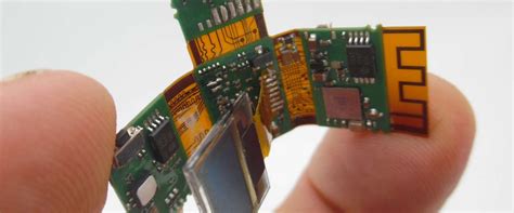
A PCB-Phone is a compact, multi-layered printed circuit board that serves as the backbone of a smartphone. It houses and interconnects various components, such as the processor, memory, sensors, and communication modules, enabling the device to perform its intended functions. The PCB-Phone is designed to optimize space utilization, signal integrity, and power efficiency, making it an essential component in the development of high-performance, feature-rich smartphones.
The Evolution of PCB-Phone Technology
The PCB-Phone has undergone significant advancements over the years, paralleling the rapid progress in mobile phone technology. As smartphones have become more sophisticated, with increased functionality and miniaturization, the PCB-Phone has adapted to accommodate these changes.
| Generation | PCB-Phone Features |
|---|---|
| 1G | Simple, single-layer PCBs for basic call functionality |
| 2G | Introduction of multi-layer PCBs for improved signal routing and component integration |
| 3G | High-density interconnect (HDI) PCBs for enhanced performance and miniaturization |
| 4G | Advanced HDI PCBs with embedded components and fine-pitch ball grid arrays (BGAs) |
| 5G | Ultra-high-density PCBs with advanced materials and packaging technologies for high-speed, low-latency communication |
PCB-Phone Manufacturing Process
The manufacturing process of a PCB-Phone involves several intricate steps to ensure the highest quality and reliability. Let’s explore each stage in detail.
1. PCB Design and Layout
The first step in PCB-Phone manufacturing is the design and layout of the circuit board. This process involves the following sub-steps:
Schematic Design
Engineers create a schematic diagram that represents the electrical connections and components required for the smartphone’s functionality. This schematic serves as a blueprint for the PCB layout.
Component Placement
The components are strategically placed on the PCB layout to optimize space utilization, signal integrity, and thermal management. Designers use advanced PCB layout software to ensure optimal component placement.
Signal Routing
The electrical connections between components are established through the routing of conductive traces on the PCB. Signal routing is a critical aspect of PCB-Phone design, as it directly affects the device’s performance and signal integrity.
2. PCB Fabrication
Once the PCB layout is finalized, the fabrication process begins. This stage involves the following steps:
Material Selection
The choice of PCB material is crucial for the performance and reliability of the PCB-Phone. Common materials used include FR-4, a glass-reinforced epoxy laminate, and high-frequency materials like Rogers RO4000 series for RF applications.
Lamination
The PCB layers are laminated together using heat and pressure to form a solid, multi-layer structure. The number of layers in a PCB-Phone can vary depending on the complexity of the design, ranging from 4 to 12 layers or more.
Drilling and Plating
Holes are drilled through the laminated PCB to accommodate component leads and vias. These holes are then plated with a conductive material, typically copper, to establish electrical connections between layers.
Etching
The unwanted copper is removed from the PCB surface using a chemical etching process, leaving only the desired conductive traces and pads.
3. Component Assembly
After the PCB fabrication is complete, the components are assembled onto the board. This stage involves the following steps:
Solder Paste Application
A precise amount of solder paste is applied to the component pads using a stencil printing process. The solder paste serves as a bonding agent between the components and the PCB.
Component Placement
The components are placed onto the PCB using automated pick-and-place machines. These machines are programmed to accurately position each component based on the PCB layout.
Reflow Soldering
The PCB with the placed components undergoes a reflow soldering process, where the board is heated to melt the solder paste and form a permanent electrical and mechanical bond between the components and the PCB.
4. Testing and Inspection
To ensure the quality and functionality of the PCB-Phone, several testing and inspection procedures are carried out:
Automated Optical Inspection (AOI)
AOI systems use high-resolution cameras and advanced image processing algorithms to detect any surface-level defects, such as missing components, solder bridging, or incorrect component placement.
In-Circuit Testing (ICT)
ICT is performed to verify the electrical connectivity and functionality of individual components on the PCB. This test helps identify any short circuits, open circuits, or component failures.
Functional Testing
The assembled PCB-Phone undergoes functional testing to ensure that all the features and functions of the smartphone are working as intended. This test covers aspects such as display, touch input, audio, camera, and wireless communication.

The Importance of PCB-Phone in Mobile Phone Industry
The PCB-Phone plays a vital role in the mobile phone industry, enabling the development of advanced, feature-rich smartphones. Let’s explore the significance of PCB-Phone technology in various aspects of the industry.
Enabling Miniaturization
One of the key advantages of PCB-Phone technology is its ability to enable the miniaturization of smartphones. By using high-density interconnect (HDI) PCBs and advanced packaging techniques, manufacturers can integrate more functionality into smaller form factors. This allows for the development of sleek, compact devices that are both portable and powerful.
Enhancing Performance
The PCB-Phone is designed to optimize signal integrity and power efficiency, leading to enhanced performance in smartphones. Advanced PCB materials and layout techniques help minimize signal loss, crosstalk, and electromagnetic interference (EMI), ensuring reliable and high-speed data transmission. Additionally, efficient power management techniques implemented on the PCB-Phone contribute to improved battery life and overall device performance.
Facilitating Innovation
The advancements in PCB-Phone technology have opened up new possibilities for innovation in the mobile phone industry. The ability to integrate multiple functions and components onto a single PCB has enabled the development of cutting-edge features such as high-resolution cameras, 5G connectivity, and advanced biometric sensors. As PCB-Phone technology continues to evolve, it will drive further innovation and shape the future of smartphones.
Cost Optimization
The PCB-Phone manufacturing process has undergone significant improvements in terms of efficiency and automation. Advanced manufacturing techniques, such as high-speed pick-and-place machines and automated optical inspection systems, have streamlined the production process, reducing manufacturing time and costs. This cost optimization enables smartphone manufacturers to offer feature-rich devices at competitive prices, making advanced technology more accessible to consumers.

Frequently Asked Questions (FAQ)
-
What is the difference between a regular PCB and a PCB-Phone?
A PCB-Phone is a specialized type of PCB designed specifically for use in smartphones. It features high-density interconnects, advanced materials, and optimized layouts to meet the unique requirements of mobile devices, such as miniaturization, performance, and power efficiency. Regular PCBs, on the other hand, are more general-purpose and may not have the same level of complexity or specialized features. -
How many layers are typically found in a PCB-Phone?
The number of layers in a PCB-Phone can vary depending on the complexity of the smartphone design. Modern smartphones often utilize PCBs with 8 to 12 layers, although some high-end devices may feature PCBs with even more layers. The increased number of layers allows for better signal routing, component integration, and overall performance. -
What are the challenges in PCB-Phone manufacturing?
PCB-Phone manufacturing poses several challenges due to the complexity and precision required. Some of the key challenges include: - Achieving high-density interconnects and fine-pitch component placement
- Ensuring signal integrity and minimizing electromagnetic interference
- Managing thermal dissipation and power efficiency
-
Maintaining high yield rates and quality control throughout the manufacturing process
-
How does the PCB-Phone contribute to the development of 5G smartphones?
The PCB-Phone plays a crucial role in enabling 5G functionality in smartphones. 5G networks require high-speed, low-latency data transmission, which demands advanced PCB materials and designs. PCB-Phones for 5G smartphones feature ultra-high-density interconnects, specialized RF materials, and optimized signal routing to ensure reliable and efficient 5G performance. -
What is the future outlook for PCB-Phone technology?
As the mobile phone industry continues to evolve, PCB-Phone technology is expected to keep pace with the increasing demands for performance, functionality, and miniaturization. Future advancements in PCB-Phone technology may include: - The use of advanced materials, such as low-loss dielectrics and high-conductivity metals
- Further miniaturization and integration of components, such as system-on-chip (SoC) and package-on-package (PoP) solutions
- Improved thermal management techniques to handle the increased power density in compact devices
- Adoption of advanced manufacturing processes, such as 3D printing and embedded component technology

Conclusion
The PCB-Phone is a critical component in the development and advancement of modern smartphones. Its specialized design, manufacturing process, and continuous evolution have enabled the mobile phone industry to push the boundaries of performance, functionality, and miniaturization. As PCB-Phone technology continues to progress, it will play a pivotal role in shaping the future of smartphones, driving innovation, and delivering cutting-edge features to consumers worldwide.
Word count: 1554


Leave a Reply