Introduction to PCB Design Rules
Printed Circuit Board (PCB) design is a complex process that involves creating an electronic circuit on a flat insulating substrate. PCB design rules are a set of guidelines and constraints that ensure the manufacturability, reliability, and functionality of the PCB. These rules are based on the capabilities of the manufacturing process, the electrical requirements of the components, and the environmental conditions in which the PCB will operate.
Following PCB design rules is crucial for several reasons:
- Manufacturability: Adhering to design rules ensures that the PCB can be manufactured using standard processes and equipment, reducing the risk of production delays and cost overruns.
- Reliability: Well-designed PCBs that follow design rules are less likely to experience failures due to manufacturing defects, component incompatibility, or environmental factors.
- Functionality: PCB design rules help ensure that the electronic circuit functions as intended by maintaining signal integrity, minimizing crosstalk, and preventing electromagnetic interference (EMI).
In this article, we will discuss the various aspects of PCB design rules, including layout guidelines, component placement, routing constraints, and manufacturing considerations.
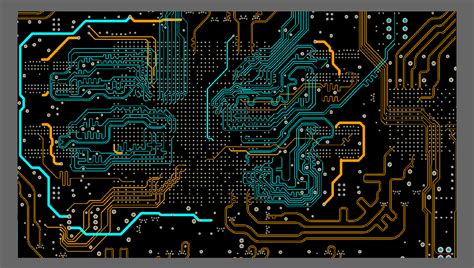
PCB Layout Guidelines
Board Size and Shape
The size and shape of the PCB are determined by the space constraints of the final product and the placement of components. When designing the board outline, consider the following:
- Ensure that the board fits within the allocated space in the product enclosure.
- Provide sufficient clearance around the board edges for mounting holes and connectors.
- Consider the placement of components, especially those with specific orientation requirements (e.g., connectors, switches, and displays).
Layer Stack-up
The layer stack-up refers to the arrangement of copper layers and insulating substrates in the PCB. A typical stack-up consists of alternating layers of copper and insulation, with the outermost layers being used for component placement and the inner layers for signal routing and power distribution.
| Layer | Description |
|---|---|
| Top | Component placement, signal routing |
| Inner | Signal routing, power distribution |
| Bottom | Component placement, signal routing |
When designing the layer stack-up, consider the following:
- Use an even number of layers to balance the board and minimize warping.
- Provide sufficient insulation between layers to prevent short circuits and signal crosstalk.
- Use dedicated layers for power distribution and ground planes to minimize noise and improve signal integrity.
Component Placement
Component placement is a critical aspect of PCB design, as it affects signal routing, thermal management, and mechanical stress. When placing components on the board, consider the following:
- Group related components together to minimize signal trace lengths and improve signal integrity.
- Place components on a grid to facilitate automated assembly and reduce manufacturing costs.
- Orient components to minimize the number of rotations required during assembly.
- Provide sufficient clearance between components to allow for signal routing and prevent short circuits.

Signal Routing Constraints
Trace Width and Spacing
Trace width and spacing are critical parameters that affect signal integrity and manufacturability. When designing signal traces, consider the following:
- Use appropriate trace widths based on the current carrying requirements of the signal.
- Maintain sufficient spacing between traces to prevent short circuits and minimize crosstalk.
- Follow the manufacturer’s recommendations for minimum trace width and spacing based on the chosen PCB fabrication process.
| Signal Type | Trace Width (mil) | Trace Spacing (mil) |
|---|---|---|
| Digital | 5-10 | 5-10 |
| Analog | 10-20 | 10-20 |
| Power | 20-50 | 20-50 |
Via Design
Vias are used to connect signal traces between layers in the PCB. When designing vias, consider the following:
- Use appropriate via sizes based on the current carrying requirements and the PCB fabrication process.
- Provide sufficient spacing between vias to prevent short circuits and minimize signal coupling.
- Use via stitching to improve signal integrity and reduce EMI.
Length Matching
Length matching is the process of ensuring that signal traces within a group have the same electrical length to minimize signal skew and maintain signal integrity. When designing for length matching, consider the following:
- Identify signal groups that require length matching, such as high-speed interfaces and differential pairs.
- Use serpentine routing or adjust trace widths to equalize the electrical lengths of the traces within a group.
- Verify the length matching using signal integrity simulations or measurements.

Manufacturing Considerations
Design for Manufacturing (DFM)
DFM is the process of designing a PCB that is easy to manufacture, test, and assemble. When designing for manufacturability, consider the following:
- Adhere to the manufacturer’s design rules for minimum feature sizes, clearances, and tolerances.
- Provide fiducial markers and assembly guides to facilitate automated assembly.
- Use standard component sizes and packages to minimize custom parts and reduce sourcing costs.
Panelization
Panelization is the process of arranging multiple PCBs on a single panel for fabrication and assembly. When designing for panelization, consider the following:
- Provide sufficient spacing between boards to allow for cutting and separation.
- Include tooling holes and fiducial markers for panel alignment and registration.
- Verify that the panel layout complies with the manufacturer’s specifications.
Testing and Inspection
Testing and inspection are critical steps in ensuring the quality and reliability of the manufactured PCBs. When designing for testing and inspection, consider the following:
- Provide test points and probe pads for in-circuit testing and debugging.
- Include bare-board testing features, such as continuity and isolation tests.
- Specify the required testing and inspection procedures in the manufacturing documentation.

Frequently Asked Questions (FAQ)
-
What are the most important PCB design rules to follow?
The most important PCB design rules include maintaining appropriate trace widths and spacings, providing sufficient clearances between components, following DFM guidelines, and ensuring signal integrity through proper routing and length matching. -
How do I choose the appropriate trace width for my PCB design?
Trace width is determined by the current carrying requirements of the signal and the PCB fabrication process. Consult the manufacturer’s design guidelines and use PCB design software to calculate the appropriate trace widths based on the electrical requirements. -
What is the purpose of length matching in PCB design?
Length matching ensures that signal traces within a group have the same electrical length, minimizing signal skew and maintaining signal integrity. This is particularly important for high-speed interfaces and differential pairs. -
How can I ensure that my PCB design is manufacturable?
To ensure manufacturability, follow the manufacturer’s DFM guidelines, use standard component sizes and packages, provide fiducial markers and assembly guides, and verify that the design complies with the fabrication process capabilities. -
What are some common PCB design mistakes to avoid?
Common PCB design mistakes include using inappropriate trace widths and spacings, neglecting signal integrity considerations, ignoring DFM guidelines, and failing to provide sufficient testing and inspection features.
Conclusion
PCB design rules are essential for creating reliable, functional, and manufacturable electronic circuits. By following layout guidelines, adhering to signal routing constraints, and considering manufacturing requirements, designers can ensure that their PCBs meet the desired performance and quality standards.
Effective PCB design requires a combination of technical knowledge, attention to detail, and collaboration with manufacturers and assembly partners. By staying up-to-date with industry best practices and leveraging PCB design software tools, designers can streamline the design process and minimize the risk of costly mistakes.
As electronic products continue to evolve and become more complex, the importance of PCB design rules will only continue to grow. By embracing these rules and adapting to new technologies and manufacturing processes, designers can create innovative and reliable electronic solutions that meet the needs of today’s increasingly connected world.


Leave a Reply