Introduction to Plated-through Holes
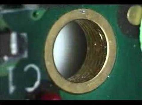
Plated-through holes (PTHs) are an essential component of printed circuit boards (PCBs) that enable electrical connectivity between different layers of the board. These holes are drilled through the PCB and then electroplated with a conductive material, typically copper, to create a reliable electrical connection. PTHs play a crucial role in the functionality and reliability of PCBs, making them a critical aspect of electronic design and manufacturing.
The Importance of Plated-through Holes
PTHs serve several important functions in PCBs:
- Electrical Connectivity: PTHs provide a conductive pathway between different layers of the PCB, allowing signals and power to be routed efficiently.
- Component Mounting: PTHs are used to mount through-hole components, such as resistors, capacitors, and connectors, to the PCB.
- Mechanical Strength: PTHs provide mechanical support and stability to the PCB, particularly when subject to stress or vibration.
- Heat Dissipation: PTHs can help dissipate heat generated by components, improving the overall thermal performance of the PCB.
The Manufacturing Process of Plated-through Holes
The creation of PTHs involves several steps in the PCB manufacturing process:
Drilling
The first step in creating PTHs is drilling holes through the PCB substrate. This is typically done using high-speed, computer-controlled drilling machines that can precisely position and drill holes of various sizes. The drilling process can be optimized to minimize the risk of defects, such as burrs or rough hole walls, which can affect the quality of the plating.
Desmearing
After drilling, the holes may contain debris and resin smear, which can impede the plating process. Desmearing involves removing this debris and preparing the hole walls for plating. This can be done through various methods, such as plasma etching, chemical desmearing, or mechanical abrasion.
Electroless Copper Deposition
Once the holes are cleaned and prepared, they are subjected to an electroless copper deposition process. This involves immersing the PCB in a copper plating solution that contains a reducing agent, which causes the copper to adhere to the hole walls without the need for an external electrical current. This initial layer of copper provides a conductive base for the subsequent electroplating process.
Electroplating
After the electroless copper deposition, the PCB undergoes an electroplating process to build up the thickness of the copper in the holes. This involves applying an electrical current to the PCB while it is immersed in a copper plating solution. The current causes the copper ions in the solution to be attracted to the hole walls, where they are reduced to metallic copper, increasing the thickness of the plating.
Inspection and Quality Control
Throughout the manufacturing process, various inspection and quality control measures are employed to ensure the integrity and reliability of the PTHs. This may include visual inspection, electrical testing, and cross-sectional analysis to verify the plating thickness and uniformity.

Design Considerations for Plated-through Holes
When designing PCBs with PTHs, several factors must be considered to ensure optimal performance and manufacturability:
Hole Size and Aspect Ratio
The size of the PTHs and their aspect ratio (the ratio of hole depth to diameter) can affect the quality and reliability of the plating. Smaller holes with higher aspect ratios are more challenging to plate uniformly and may be more susceptible to defects. Designers should consider the capabilities of their manufacturing partners and adhere to recommended guidelines for hole sizes and aspect ratios.
Pad Size and Annular Ring
The pad size and annular ring (the copper area surrounding the hole on the PCB surface) play a role in the mechanical strength and electrical connectivity of the PTH. Larger pads and annular rings provide more surface area for the plating to adhere to, improving the reliability of the connection. However, designers must balance this with the overall space constraints and routing requirements of the PCB.
Plating Thickness and Material
The thickness and material of the PTH plating can impact its electrical and mechanical properties. Thicker plating can improve the current-carrying capacity and mechanical strength of the PTH, but may also increase the cost and manufacturing complexity. The choice of plating material, such as copper or gold, will depend on the specific requirements of the application, such as conductivity, corrosion resistance, and solderability.
Thermal Management
PTHs can serve as thermal pathways, helping to dissipate heat from components mounted on the PCB. Designers should consider the thermal requirements of their components and strategically place PTHs to promote heat transfer and minimize thermal stress on the PCB.

Common Plated-through Hole Defects and Their Causes
Despite advances in manufacturing processes and quality control, PTHs can still be subject to various defects that can affect the performance and reliability of the PCB. Some common PTH defects include:
Voids
Voids are gaps or holes in the plating that can occur due to inadequate cleaning, air bubbles in the plating solution, or insufficient plating thickness. Voids can reduce the electrical conductivity and mechanical strength of the PTH, potentially leading to failures.
Nodules
Nodules are small, raised bumps on the surface of the PTH plating that can occur due to contaminants in the plating solution or excessive current density during electroplating. Nodules can interfere with the solderability and electrical contact of the PTH.
Cracks
Cracks in the PTH plating can occur due to thermal stress, mechanical stress, or poor plating adhesion. Cracks can compromise the electrical conductivity and mechanical integrity of the PTH, leading to intermittent failures or open circuits.
Thin or Uneven Plating
Thin or uneven plating can result from inadequate plating time, poor solution maintenance, or uneven current distribution during electroplating. Thin or uneven plating can reduce the current-carrying capacity and mechanical strength of the PTH, making it more susceptible to failure under stress.
To minimize the occurrence of these defects, manufacturers must adhere to strict process controls, regularly maintain and monitor their plating solutions, and employ robust inspection and testing procedures to catch defects early in the manufacturing process.

Advancements in Plated-through Hole Technology
As PCB designs continue to push the boundaries of miniaturization and performance, new technologies and processes are being developed to improve the capabilities and reliability of PTHs:
High Aspect Ratio Plating
High aspect ratio plating techniques, such as reverse pulse plating or periodic pulse reverse plating, enable the uniform plating of holes with aspect ratios greater than 10:1. These techniques use specialized waveforms and plating chemistries to promote even current distribution and minimize the formation of voids or nodules.
Filled Plated-through Holes
Filled PTHs involve filling the plated hole with a non-conductive material, such as epoxy or resin, to improve the mechanical strength and thermal performance of the PTH. This can be particularly beneficial for high-density PCBs or those subject to extreme mechanical or thermal stress.
Via-in-Pad Technology
Via-in-pad technology allows PTHs to be placed directly in the component pads, saving space and enabling higher-density PCB designs. This requires precise control over the plating process to ensure a smooth, planar surface for component mounting.
Microvias
Microvias are small, laser-drilled holes that can be used to create high-density interconnects between layers in a PCB. These vias typically have diameters less than 150 microns and can be filled with conductive or non-conductive materials to improve reliability and signal integrity.
Conclusion
Plated-through holes are a critical component of PCBs, providing electrical connectivity, mechanical support, and thermal management. The manufacturing process of PTHs involves precise drilling, cleaning, and plating steps to ensure reliable and consistent performance. Designers must consider various factors, such as hole size, pad size, and plating thickness, to optimize the functionality and manufacturability of their PCBs.
As PCB technology continues to advance, new techniques and processes are being developed to improve the capabilities and reliability of PTHs. By understanding the fundamentals of PTHs and staying informed about the latest advancements, designers and manufacturers can create PCBs that push the boundaries of performance and reliability.
Frequently Asked Questions (FAQ)
1. What is the purpose of plated-through holes in PCBs?
Plated-through holes serve several purposes in PCBs, including providing electrical connectivity between layers, allowing the mounting of through-hole components, offering mechanical support, and aiding in heat dissipation.
2. What materials are used for plating through-holes?
The most common material used for plating through-holes is copper. However, other materials, such as gold or silver, may be used for specific applications that require enhanced conductivity or corrosion resistance.
3. How does the aspect ratio of a plated-through hole affect its manufacturability?
The aspect ratio of a plated-through hole, which is the ratio of its depth to its diameter, can impact the manufacturability of the hole. Higher aspect ratios (deeper holes with smaller diameters) are more challenging to plate uniformly and may be more susceptible to defects like voids or thin plating.
4. What are some common defects that can occur in plated-through holes?
Common defects in plated-through holes include voids (gaps in the plating), nodules (raised bumps on the plating surface), cracks, and thin or uneven plating. These defects can be caused by various factors, such as inadequate cleaning, contaminants in the plating solution, or uneven current distribution during electroplating.
5. What advancements have been made in plated-through hole technology?
Recent advancements in plated-through hole technology include high aspect ratio plating techniques, filled plated-through holes, via-in-pad technology, and microvias. These innovations aim to improve the capabilities and reliability of PTHs, enabling higher-density PCB designs and better performance under demanding conditions.
| Plated-through Hole Defect | Causes | Effects |
|---|---|---|
| Voids | – Inadequate cleaning – Air bubbles in plating solution – Insufficient plating thickness |
– Reduced electrical conductivity – Reduced mechanical strength – Potential failures |
| Nodules | – Contaminants in plating solution – Excessive current density during electroplating |
– Interference with solderability – Interference with electrical contact |
| Cracks | – Thermal stress – Mechanical stress – Poor plating adhesion |
– Compromised electrical conductivity – Compromised mechanical integrity – Intermittent failures or open circuits |
| Thin or Uneven Plating | – Inadequate plating time – Poor solution maintenance – Uneven current distribution during electroplating |
– Reduced current-carrying capacity – Reduced mechanical strength – Increased susceptibility to failure under stress |


Leave a Reply