Introduction to PCBA Testing
Printed Circuit Board Assembly (PCBA) is a crucial process in the manufacturing of electronic devices. To ensure the quality and reliability of the final product, various test and inspection methods are employed at different stages of the assembly process. These methods help identify defects, ensure proper functionality, and maintain the highest standards of quality control. In this article, we will explore several PCBA test and inspection methods, their importance, and their application in the manufacturing process.
Visual Inspection
Manual Visual Inspection
One of the most basic and essential methods of PCBA testing is manual visual inspection. This process involves trained technicians carefully examining the assembled PCB for any visible defects, such as:
- Incorrect component placement
- Solder bridges or shorts
- Insufficient or excessive solder
- Damaged or missing components
Manual visual inspection is often performed at various stages of the assembly process, including pre-soldering, post-soldering, and final inspection. While this method is relatively simple and cost-effective, it is subject to human error and may not detect more subtle defects.
Automated Optical Inspection (AOI)
To overcome the limitations of manual visual inspection, Automated Optical Inspection (AOI) systems are widely used in PCBA testing. AOI machines use high-resolution cameras and advanced image processing algorithms to scan the assembled PCB for defects. These systems can detect a wide range of issues, including:
- Component placement errors
- Solder defects (bridges, insufficient solder, etc.)
- Incorrect component polarity or orientation
- Damaged or missing components
AOI systems offer several advantages over manual inspection, such as:
- Higher speed and throughput
- Increased accuracy and consistency
- Ability to detect subtle defects
- Reduced labor costs
However, AOI systems may struggle with certain types of defects, such as those hidden under components or within connectors.

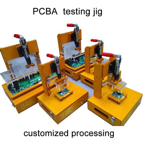
In-Circuit Testing (ICT)
In-Circuit Testing (ICT) is a powerful method for verifying the functionality and connectivity of individual components on the assembled PCB. ICT involves using a bed-of-nails fixture, which consists of an array of spring-loaded pins that make contact with specific test points on the PCB. The test system then applies electrical signals to these test points and measures the response to determine if the components are functioning correctly and are properly connected.
ICT can detect a variety of defects, including:
- Open or short circuits
- Incorrect component values (resistors, capacitors, etc.)
- Missing or incorrectly placed components
- Defective integrated circuits
Advantages of ICT include:
- High fault coverage
- Ability to test both analog and digital components
- Fast and automated testing process
However, ICT requires a custom-designed test fixture for each PCB design, which can be expensive and time-consuming to develop. Additionally, ICT may not be suitable for certain types of components or high-density PCBs with limited access to test points.

Flying Probe Testing
Flying Probe Testing is an alternative to ICT that does not require a custom bed-of-nails fixture. Instead, this method uses a set of movable probes that can be programmed to contact specific test points on the PCB. The probes then apply electrical signals and measure the response, similar to ICT.
Flying Probe Testing offers several advantages, including:
- Flexibility: The same machine can be used to test different PCB designs without requiring a custom fixture.
- Ability to test high-density PCBs: The movable probes can access test points that may be difficult or impossible to reach with a bed-of-nails fixture.
- Lower upfront costs: Since no custom fixture is required, the initial investment in Flying Probe Testing equipment is often lower than ICT.
However, Flying Probe Testing is generally slower than ICT, as the probes must move from one test point to another. Additionally, the programming and setup time for Flying Probe Testing can be significant.

Functional Testing
Functional Testing is a critical step in PCBA testing that verifies the overall functionality and performance of the assembled PCB. This method involves applying power to the board and testing its various functions, such as:
- Input/output connectivity
- Communication interfaces
- Display and user interface elements
- Sensors and actuators
- Power management and regulation
Functional Testing often requires custom-designed test fixtures and software to simulate the PCB’s intended operating environment. This method can detect defects and issues that may not be apparent during earlier stages of testing, such as:
- Incorrect component values or tolerances
- Timing or signal integrity issues
- Firmware or software bugs
- Thermal or power-related problems
Advantages of Functional Testing include:
- Verification of end-to-end functionality
- Ability to detect complex and interrelated issues
- Increased confidence in the final product quality
However, Functional Testing can be time-consuming and expensive, requiring significant investment in test equipment and engineering resources.
Boundary Scan Testing
Boundary Scan Testing, also known as JTAG (Joint Test Action Group) testing, is a method for testing the interconnections and functionality of digital components on a PCB. This method relies on a special design feature called boundary scan cells, which are built into the components themselves.
During Boundary Scan Testing, a test system communicates with the boundary scan cells through a standard interface (JTAG) and can:
- Read and write data to the component’s input and output pins
- Control the component’s internal state and functionality
- Verify the connectivity between components
Advantages of Boundary Scan Testing include:
- Ability to test complex digital components and interconnections
- High fault coverage for digital circuits
- Reduced need for physical test access points
- Standardized test interface (JTAG)
However, Boundary Scan Testing is limited to digital components with built-in boundary scan support and may not cover analog or mixed-signal portions of the PCB.
X-Ray Inspection
X-Ray Inspection is a non-destructive testing method that uses X-rays to create images of the internal structure of the assembled PCB. This method is particularly useful for detecting defects that are hidden from view, such as:
- Voids or inclusions in solder joints
- Broken or damaged traces within the PCB
- Incorrectly seated or aligned BGA (Ball Grid Array) components
X-Ray Inspection systems can be either 2D or 3D, with 3D systems providing more detailed and accurate images of the PCB’s internal structure.
Advantages of X-Ray Inspection include:
- Ability to detect defects that are not visible to the naked eye or optical inspection systems
- Non-destructive nature, allowing for testing of production PCBs
- Detailed imaging of complex and high-density PCB structures
However, X-Ray Inspection equipment can be expensive, and the interpretation of the resulting images requires skilled technicians. Additionally, X-Ray Inspection may not detect all types of defects, such as those related to component functionality or performance.
Frequently Asked Questions (FAQ)
-
Q: What is the difference between manual visual inspection and automated optical inspection (AOI)?
A: Manual visual inspection relies on trained technicians to visually examine the PCB for defects, while AOI uses high-resolution cameras and image processing algorithms to automatically detect defects. AOI is faster, more consistent, and can detect subtle defects that may be missed by manual inspection. -
Q: Can In-Circuit Testing (ICT) detect all types of defects on a PCB?
A: While ICT is a powerful method for detecting a wide range of defects, it may not be suitable for certain types of components or high-density PCBs with limited access to test points. Additionally, ICT primarily focuses on the functionality and connectivity of individual components and may not detect issues related to overall system performance or functionality. -
Q: Is Flying Probe Testing faster than In-Circuit Testing (ICT)?
A: In general, Flying Probe Testing is slower than ICT because the probes must move from one test point to another, whereas ICT can test multiple points simultaneously using a bed-of-nails fixture. However, Flying Probe Testing offers greater flexibility and lower upfront costs compared to ICT. -
Q: What types of defects can Functional Testing detect that other methods may miss?
A: Functional Testing can detect defects and issues related to the overall performance and functionality of the PCB, such as incorrect component values or tolerances, timing or signal integrity issues, firmware or software bugs, and thermal or power-related problems. These issues may not be apparent during earlier stages of testing that focus on individual components or interconnections. -
Q: Is X-Ray Inspection a destructive testing method?
A: No, X-Ray Inspection is a non-destructive testing method. It uses X-rays to create detailed images of the PCB’s internal structure without causing any damage to the board or components. This allows for the testing of production PCBs without compromising their integrity or functionality.
Conclusion
PCBA testing and inspection are critical processes in ensuring the quality, reliability, and functionality of electronic devices. By employing a combination of methods, including visual inspection, automated optical inspection, in-circuit testing, flying probe testing, functional testing, boundary scan testing, and X-ray inspection, manufacturers can detect and address a wide range of defects and issues.
Each testing method has its own advantages and limitations, and the choice of methods depends on factors such as the complexity of the PCB, the types of components used, and the desired level of fault coverage. By understanding the strengths and weaknesses of each method and applying them appropriately, manufacturers can optimize their testing processes and ensure the highest quality standards for their products.
As electronic devices continue to become more complex and miniaturized, the importance of effective PCBA testing and inspection will only continue to grow. By staying up-to-date with the latest testing technologies and best practices, manufacturers can maintain a competitive edge and deliver products that meet the ever-increasing demands of consumers and businesses alike.


Leave a Reply