What is PCB Burn-in Testing?
PCB burn-in testing is a critical process in the manufacturing of printed circuit boards (PCBs) that involves subjecting the boards to elevated temperatures and voltages for an extended period to identify and eliminate early-life failures. This process is designed to stress the components and connections on the PCB, accelerating the aging process and revealing any defects or weaknesses that may cause problems during normal operation.
The primary goal of PCB burn-in testing is to improve the reliability and longevity of the final product by weeding out defective components and ensuring that only high-quality PCBs are shipped to customers. By detecting and addressing issues early in the manufacturing process, manufacturers can reduce warranty claims, minimize field failures, and enhance customer satisfaction.
Types of PCB Burn-in Testing
There are two main types of PCB burn-in testing:
-
Static Burn-in Testing: In this method, the PCB is subjected to elevated temperatures and voltages without any active components or power cycling. The board is simply placed in a controlled environment and monitored for any signs of failure or degradation.
-
Dynamic Burn-in Testing: This method involves actively exercising the PCB’s components and circuits while subjecting the board to elevated temperatures and voltages. The PCB is powered on and off, and various test signals are applied to simulate real-world operating conditions.
The PCB Burn-in Testing Process
The PCB burn-in testing process typically consists of several stages, each designed to stress the board and its components in different ways. The following is a general overview of the process:
1. Test Setup and Preparation
Before the actual burn-in testing can begin, the PCB must be properly prepared and set up in the testing environment. This involves:
- Cleaning the PCB to remove any contaminants or debris that could interfere with the testing process.
- Attaching the necessary test probes, connectors, and monitoring equipment to the PCB.
- Configuring the burn-in chamber or oven to the desired temperature and voltage settings.
2. Temperature and Voltage Stressing
Once the PCB is set up, it is subjected to elevated temperatures and voltages for a predetermined period. The specific temperature and voltage levels used depend on the type of PCB being tested and the requirements of the end application.
Typical burn-in testing conditions include:
| Parameter | Range |
|---|---|
| Temperature | 85°C to 125°C |
| Voltage | 1.2 to 1.5 times the nominal operating voltage |
| Duration | 24 to 168 hours |
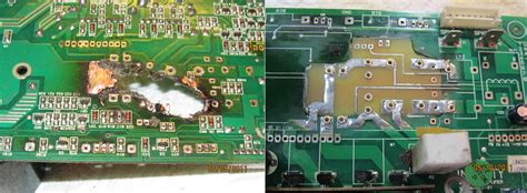
During this stage, the PCB is continuously monitored for any signs of failure or degradation, such as short circuits, open circuits, or component malfunctions.
3. Functional Testing
After the temperature and voltage stressing stage, the PCB undergoes functional testing to verify that all components and circuits are operating correctly. This may involve applying various test signals to the board and measuring the response, as well as performing visual inspections to check for any physical damage or defects.
Functional testing may include:
- Continuity testing to verify that all connections are intact and properly formed.
- Resistance testing to check for any changes in the electrical properties of the components or traces.
- Signal integrity testing to ensure that the PCB can properly transmit and receive signals without distortion or interference.
4. Data Analysis and Reporting
Throughout the burn-in testing process, data is collected and analyzed to identify any trends or patterns that may indicate potential issues or failures. This data is used to generate detailed reports on the performance and reliability of the PCB, which can be used to make informed decisions about the manufacturing process and product design.
Some key metrics that may be included in a burn-in testing report include:
- Failure rates and types
- Time-to-failure statistics
- Component-level performance data
- Environmental conditions (temperature, humidity, etc.)

Benefits of PCB Burn-in Testing
Implementing a comprehensive PCB burn-in testing process offers several key benefits for manufacturers and end-users alike:
-
Improved Reliability: By identifying and eliminating early-life failures, burn-in testing helps to ensure that only high-quality, reliable PCBs are shipped to customers. This can significantly reduce the risk of field failures and warranty claims, leading to lower overall costs and enhanced customer satisfaction.
-
Increased Product Lifespan: PCBs that have undergone burn-in testing are more likely to operate reliably over their intended lifespan, as the testing process helps to weed out components and boards that are prone to premature failure. This can lead to longer-lasting, more dependable products that require fewer repairs or replacements.
-
Enhanced Quality Control: Burn-in testing provides valuable data and insights into the manufacturing process, allowing manufacturers to identify and address any issues or inconsistencies that may be affecting product quality. By continuously monitoring and analyzing test results, manufacturers can implement process improvements and ensure that their PCBs meet or exceed industry standards.
-
Cost Savings: While burn-in testing does require an initial investment in equipment and resources, it can ultimately lead to significant cost savings by reducing the number of defective PCBs that make it to the end-user. This can help to minimize warranty claims, field service costs, and product recalls, all of which can have a major impact on a company’s bottom line.
-
Compliance with Industry Standards: Many industries, such as automotive, aerospace, and medical devices, have strict reliability and quality requirements for PCBs. By incorporating burn-in testing into their manufacturing process, companies can demonstrate compliance with these standards and gain a competitive edge in the marketplace.

Challenges and Considerations
While PCB burn-in testing offers numerous benefits, there are also some challenges and considerations that manufacturers must take into account:
-
Cost and Time: Burn-in testing can be a time-consuming and resource-intensive process, requiring specialized equipment and skilled personnel. Manufacturers must carefully balance the costs and benefits of the testing process to ensure that it is financially viable and does not unduly impact production schedules.
-
Component Compatibility: Not all components are designed to withstand the elevated temperatures and voltages used in burn-in testing. Manufacturers must carefully select components that are rated for the intended testing conditions and ensure that they are properly mounted and protected during the process.
-
Test Coverage: Burn-in testing cannot guarantee that a PCB will be completely free of defects or failures, as some issues may only manifest under specific operating conditions or after extended use. Manufacturers must carefully design their testing protocols to provide adequate coverage and minimize the risk of undetected failures.
-
Overdesign: In some cases, manufacturers may be tempted to overdesign their PCBs to increase the likelihood of passing burn-in testing. However, this can lead to increased costs and complexity, as well as potential performance trade-offs. It is important to strike a balance between reliability and practicality when designing PCBs for burn-in testing.

FAQ
-
Q: How long does a typical PCB burn-in test last?
A: The duration of a PCB burn-in test can vary depending on the specific requirements of the application and the type of PCB being tested. Typical burn-in tests can last anywhere from 24 to 168 hours, with some tests extending even longer for critical applications. -
Q: Can burn-in testing be performed on assembled PCBs?
A: Yes, burn-in testing can be performed on fully assembled PCBs, including those with attached components and devices. In fact, testing assembled PCBs can provide a more comprehensive assessment of the board’s overall reliability and performance. -
Q: What are the most common failure modes identified during burn-in testing?
A: Some of the most common failure modes identified during PCB burn-in testing include component failures (such as capacitor or resistor failures), solder joint defects, and trace or via failures. Other issues, such as component misalignment or incorrect polarity, may also be detected during the testing process. -
Q: Is burn-in testing required for all PCBs?
A: While burn-in testing is not required for all PCBs, it is highly recommended for applications where reliability and longevity are critical, such as in the automotive, aerospace, and medical device industries. Many manufacturers also choose to perform burn-in testing as a standard part of their quality control process to ensure the highest level of product quality and customer satisfaction. -
Q: Can burn-in testing be performed in-house, or is it typically outsourced?
A: Burn-in testing can be performed either in-house or outsourced to a specialized testing facility, depending on the manufacturer’s resources and capabilities. Many larger manufacturers have dedicated burn-in testing equipment and personnel, while smaller companies may choose to outsource the process to a third-party provider. Ultimately, the decision to perform burn-in testing in-house or outsource it will depend on factors such as cost, volume, and the complexity of the testing requirements.
Conclusion
PCB burn-in testing is a critical process in the manufacturing of high-quality, reliable printed circuit boards. By subjecting PCBs to elevated temperatures and voltages, manufacturers can identify and eliminate early-life failures, improve product longevity, and enhance customer satisfaction.
While burn-in testing does present some challenges and considerations, such as cost, time, and component compatibility, the benefits of the process far outweigh the potential drawbacks. By implementing a comprehensive burn-in testing strategy, manufacturers can ensure that their PCBs meet the highest standards of quality and reliability, while also reducing costs and minimizing the risk of field failures.
As the demand for ever-more-complex and reliable electronic devices continues to grow, the importance of PCB burn-in testing will only continue to increase. By staying at the forefront of testing technologies and best practices, manufacturers can position themselves for success in an increasingly competitive marketplace and deliver the high-quality products that their customers demand.


Leave a Reply