Introduction to PCB Stackup
PCB stackup refers to the arrangement of copper and insulating layers that make up a printed circuit board (PCB). The stackup design plays a crucial role in determining the electrical performance, signal integrity, and manufacturability of a PCB. A well-designed PCB stackup ensures proper Impedance Control, minimizes crosstalk, and reduces electromagnetic interference (EMI).
In this article, we will discuss eight essential rules for designing an effective PCB stackup. By following these guidelines, you can optimize your PCB Design and achieve better overall performance.
Rule 1: Determine the Number of Layers
Factors Affecting the Number of Layers
The first step in designing a PCB stackup is to determine the number of layers required. The number of layers depends on several factors, including:
- Circuit complexity
- Signal density
- Power requirements
- Cost constraints
Choosing the Right Number of Layers
When deciding on the number of layers, consider the following guidelines:
- Simple designs with low signal density can often be achieved with a 2-layer PCB.
- Moderate complexity designs may require a 4-layer PCB.
- High-speed designs or designs with high signal density may need 6 or more layers.
| Number of Layers | Typical Applications |
|---|---|
| 2 | Simple, low-density designs |
| 4 | Moderate complexity, medium-density designs |
| 6 or more | High-speed, high-density, or complex designs |

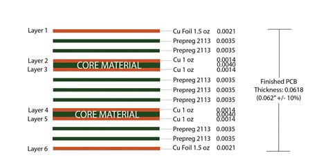
Rule 2: Choose the Right Layer Stack Sequence
Standard Layer Stack Sequences
The layer stack sequence refers to the order in which the copper and insulating layers are arranged. There are several standard layer stack sequences commonly used in PCB design:
- 2-layer: Signal – Ground
- 4-layer: Signal – Ground – Power – Signal
- 6-layer: Signal – Ground – Signal – Power – Ground – Signal
Customizing the Layer Stack Sequence
In some cases, you may need to customize the layer stack sequence to meet specific design requirements. For example:
- Placing signal layers close to the surface for high-speed designs
- Adding dedicated power planes for different voltage levels
- Incorporating shielding layers to reduce EMI

Rule 3: Select the Appropriate Dielectric Material
Common Dielectric Materials
The dielectric material is the insulating layer between the copper layers in a PCB. The choice of dielectric material affects the electrical properties and manufacturability of the PCB. Common dielectric materials include:
- FR-4: A standard, cost-effective material suitable for most applications
- Rogers: High-performance materials with low loss and stable dielectric constant
- Polyimide: Thin, flexible materials for high-density interconnects
Dielectric Properties
When selecting a dielectric material, consider the following properties:
- Dielectric constant (Dk): Affects the impedance and propagation speed of signals
- Dissipation factor (Df): Determines the amount of signal loss in the material
- Thickness: Influences the impedance and manufacturability of the PCB

Rule 4: Control Impedance
Importance of Impedance Control
Impedance control is essential for maintaining signal integrity and reducing reflections in high-speed designs. By matching the impedance of the PCB traces to the source and load impedances, you can minimize signal distortion and ensure proper signal propagation.
Factors Affecting Impedance
The impedance of a PCB trace depends on several factors:
- Trace width
- Trace thickness
- Dielectric thickness
- Dielectric constant
Calculating Impedance
To calculate the impedance of a PCB trace, you can use online calculators or specialized PCB design software. These tools take into account the various factors affecting impedance and provide guidance on trace dimensions and spacing.
Rule 5: Manage Power Distribution
Power Plane Placement
Proper power distribution is crucial for maintaining signal integrity and reducing noise in a PCB. When designing the PCB stackup, consider the following guidelines for power plane placement:
- Place power planes close to the surface layers to reduce inductance
- Use dedicated power planes for different voltage levels
- Avoid splitting power planes unless necessary for isolation
Decoupling Capacitors
Decoupling capacitors play a vital role in managing power distribution and reducing noise. To effectively use decoupling capacitors:
- Place them close to the power pins of ICs
- Use a combination of bulk and ceramic capacitors for different frequency ranges
- Minimize the loop area between the capacitor and the power/ground planes
Rule 6: Consider Signal Integrity
Crosstalk Reduction
Crosstalk occurs when signals from one trace interfere with signals on adjacent traces. To minimize crosstalk:
- Increase the spacing between traces
- Use guard traces or ground shields between sensitive signals
- Route critical traces on different layers
EMI Reduction
Electromagnetic interference (EMI) can cause signal degradation and violate regulatory requirements. To reduce EMI:
- Use ground planes to provide shielding
- Minimize the loop area of high-frequency signals
- Route high-speed signals away from the board edges
Rule 7: Optimize Via Placement
Via Types
Vias are used to connect traces on different layers of a PCB. There are several types of vias:
- Through-hole vias: Extend through all layers of the PCB
- Blind vias: Connect an Outer Layer to an inner layer
- Buried vias: Connect inner layers without reaching the outer layers
Via Placement Guidelines
When placing vias in your PCB stackup, follow these guidelines:
- Minimize the number of vias to reduce signal discontinuities
- Place vias close to the components they are connecting
- Avoid placing vias in high-speed signal paths
Rule 8: Collaborate with your Manufacturer
Manufacturing Limitations
PCB manufacturers have specific capabilities and limitations that can affect your stackup design. It’s essential to collaborate with your manufacturer early in the design process to ensure that your stackup is manufacturable and cost-effective.
Design for Manufacturability (DFM)
To optimize your PCB stackup for manufacturability:
- Follow the manufacturer’s design rules and guidelines
- Use standard layer stack sequences when possible
- Minimize the use of special materials or processes
Frequently Asked Questions (FAQ)
-
Q: What is the difference between a power plane and a ground plane?
A: A power plane is a solid copper layer that distributes a specific voltage level to the components on a PCB. A ground plane, on the other hand, provides a low-impedance return path for signals and helps to shield against EMI. -
Q: Can I mix different dielectric materials in the same PCB stackup?
A: Yes, it is possible to use different dielectric materials in the same PCB stackup. This is often done to optimize the electrical properties of specific layers or to meet certain design requirements. However, mixing dielectric materials can increase the complexity and cost of the PCB manufacturing process. -
Q: How do I determine the appropriate trace width and spacing for my PCB stackup?
A: The trace width and spacing depend on several factors, such as the signal frequency, impedance requirements, and manufacturing capabilities. You can use online calculators or PCB design software to determine the appropriate trace dimensions based on your specific design requirements. It’s also important to consult with your PCB manufacturer to ensure that your chosen trace widths and spacings are manufacturable. -
Q: What is the purpose of a blind or buried via in a PCB stackup?
A: Blind and buried vias are used to connect inner layers of a PCB without extending to the outer layers. This can be useful for reducing the overall thickness of the PCB, improving signal integrity, and minimizing the surface area occupied by vias. Blind and buried vias are typically used in high-density designs where space is limited or in situations where the outer layers need to be free of via pads for component placement or routing. -
Q: How can I ensure that my PCB stackup is compatible with my chosen manufacturing process?
A: To ensure compatibility with your chosen manufacturing process, it’s essential to collaborate with your PCB manufacturer early in the design phase. Share your stackup design with the manufacturer and ask for their feedback and recommendations. They can provide guidance on material selection, layer stack sequences, and design rules that are specific to their manufacturing capabilities. By working closely with your manufacturer, you can avoid potential issues and ensure a smooth, cost-effective production process.
Conclusion
Designing an effective PCB stackup is crucial for achieving optimal electrical performance, signal integrity, and manufacturability. By following the eight rules outlined in this article, you can create a stackup that meets your specific design requirements while minimizing potential issues.
Remember to consider factors such as the number of layers, layer stack sequence, dielectric material, impedance control, power distribution, signal integrity, via placement, and manufacturability when designing your PCB stackup. Collaborate with your PCB manufacturer throughout the design process to ensure that your stackup is compatible with their capabilities and can be efficiently produced.
By taking a comprehensive approach to PCB stackup design, you can create reliable, high-performance electronic products that meet the demands of today’s complex applications.


Leave a Reply