Introduction
Printed Circuit Board Assembly (PCBA) is a complex process that involves the integration of electronic components onto a printed circuit board (PCB). The goal is to create a functional electronic device that meets the desired specifications and performance requirements. However, during the manufacturing process, various defects can occur, leading to issues such as reduced performance, reliability, and even complete failure of the assembled board.
In this article, we will discuss seven common PCBA Manufacturing defects and provide solutions to prevent or mitigate these issues. By understanding these defects and implementing the appropriate measures, manufacturers can improve the quality of their PCBA products and reduce the associated costs of rework and scrap.
PCBA Manufacturing Process Overview
Before diving into the specific defects, let’s briefly overview the PCBA manufacturing process to provide context for the discussion.
-
PCB Fabrication: The process begins with the fabrication of the bare PCB, which involves creating the conductive traces, pads, and vias on the board substrate.
-
Solder Paste Application: Solder paste, a mixture of tiny solder particles and flux, is applied to the pads on the PCB using a stencil or screen printing process.
-
Component Placement: Surface mount devices (SMDs) and through-hole components are placed onto the PCB using automated pick-and-place machines or manual assembly methods.
-
Reflow Soldering: The populated PCB is subjected to a controlled heating process in a reflow oven, which melts the solder paste and forms a permanent electrical and mechanical connection between the components and the PCB.
-
Inspection and Testing: The assembled PCBA undergoes various inspection and testing procedures to ensure proper functionality and adherence to quality standards.

Common PCBA Manufacturing Defects and Solutions
1. Solder Bridging
Description
Solder bridging occurs when excess solder creates an unintended connection between two or more adjacent pads or traces on the PCB. This defect can lead to short circuits and malfunctioning of the assembled board.
Causes
- Excessive solder paste application
- Improper stencil design or alignment
- Incorrect reflow profile settings
- Component misalignment
Solutions
- Optimize solder paste stencil design and thickness
- Ensure proper stencil alignment during solder paste application
- Adjust reflow profile parameters (temperature, time, and conveyor speed)
- Implement automated optical inspection (AOI) to detect solder bridges
- Use solder mask between closely spaced pads to prevent bridging
2. Tombstoning
Description
Tombstoning, also known as chipstanding or drawbridging, is a defect where a surface mount component stands up on one end, forming an open circuit on one side and a solder joint on the other. This issue is most commonly observed with small, lightweight components such as chip resistors and capacitors.
Causes
- Uneven heating during the reflow process
- Imbalanced solder paste volume on component pads
- Incorrect component placement or orientation
- Inadequate adhesion between the component and solder paste
Solutions
- Ensure even heating across the PCB during reflow soldering
- Optimize solder paste stencil aperture design for balanced paste deposition
- Verify component placement accuracy and orientation
- Use solder paste with adequate tackiness to hold components in place
- Implement AOI to detect tombstoned components
3. Insufficient Solder Joints
Description
Insufficient solder joints occur when there is not enough solder to form a reliable electrical and mechanical connection between the component and the PCB pad. This defect can lead to intermittent connections, increased resistance, and potential failure of the joint over time.
Causes
- Inadequate solder paste volume
- Incorrect stencil thickness or aperture design
- Poor wetting of the solder on the component or PCB pad
- Contamination on the component leads or PCB pads
Solutions
- Optimize solder paste stencil design for adequate paste deposition
- Ensure proper storage and handling of solder paste to maintain its quality
- Verify the cleanliness of component leads and PCB pads before assembly
- Implement solder paste inspection (SPI) to monitor paste volume and consistency
- Use X-ray inspection to detect insufficient solder joints in hard-to-access areas
4. Lifted Pads
Description
Lifted pads occur when the copper pad on the PCB separates from the board substrate during the assembly process. This defect can result in broken connections, intermittent issues, and reduced reliability of the assembled board.
Causes
- Excessive heat during the reflow process
- Mechanical stress during component placement or handling
- Weak adhesion between the copper pad and PCB substrate
- Contamination or oxidation on the PCB pads
Solutions
- Optimize reflow profile to avoid excessive heat exposure
- Ensure gentle handling of the PCB during assembly to minimize mechanical stress
- Improve the adhesion between copper pads and PCB substrate through proper surface treatment and lamination processes
- Maintain cleanliness of the PCB pads and control the storage environment to prevent contamination and oxidation
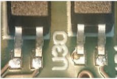
5. Component Misalignment
Description
Component misalignment refers to the improper placement of components on the PCB, where the component leads are not accurately aligned with the corresponding pads. Misaligned components can lead to poor solder joints, shorts, or opens, compromising the functionality of the assembled board.
Causes
- Incorrect component placement by the pick-and-place machine
- Inaccurate fiducial markers or reference points on the PCB
- Warpage or dimensional variations in the PCB
- Inadequate component lead coplanarity
Solutions
- Regularly calibrate and maintain pick-and-place machines for accurate component placement
- Ensure proper design and placement of fiducial markers on the PCB
- Control PCB Warpage through proper material selection and storage conditions
- Verify component lead coplanarity and packaging quality from suppliers
- Implement AOI to detect component misalignment and make necessary corrections
6. Solder Balls
Description
Solder balls are small, spherical particles of solder that can form on the PCB surface during the reflow process. These balls can cause short circuits if they come into contact with adjacent pads or traces, leading to malfunctioning of the assembled board.
Causes
- Excessive solder paste volume or improper stencil design
- Contamination or oxidation on the PCB surface
- Incorrect reflow profile settings, causing solder splatter
- Insufficient cleaning of the PCB after assembly
Solutions
- Optimize solder paste stencil design and thickness to control paste volume
- Ensure cleanliness of the PCB surface before solder paste application
- Adjust reflow profile parameters to minimize solder splatter
- Implement effective cleaning processes to remove flux residues and solder balls
- Use AOI or visual inspection to detect and remove solder balls
7. Flux Residue
Description
Flux residue is the remaining chemical substance on the PCB surface after the soldering process. While flux is necessary to promote solder wetting and prevent oxidation, excessive or unremoved flux residue can lead to corrosion, reduced insulation resistance, and potential reliability issues.
Causes
- Insufficient cleaning after the soldering process
- Use of highly active or corrosive flux
- Improper reflow profile, causing flux charring
- Inadequate ventilation during the soldering process
Solutions
- Implement effective cleaning processes to remove flux residues, such as aqueous or solvent-based cleaning
- Select flux types with lower activity levels or no-clean formulations
- Optimize reflow profile to minimize flux charring and residue formation
- Ensure adequate ventilation in the soldering area to prevent flux buildup
- Use visual inspection or ionic contamination testing to monitor flux residue levels

Frequently Asked Questions (FAQ)
1. What is the most common PCBA manufacturing defect?
The most common PCBA manufacturing defect is solder bridging, which occurs when excess solder creates an unintended connection between adjacent pads or traces on the PCB.
2. How can I prevent tombstoning of surface mount components?
To prevent tombstoning, ensure even heating across the PCB during reflow soldering, optimize solder paste stencil aperture design for balanced paste deposition, verify component placement accuracy and orientation, and use solder paste with adequate tackiness to hold components in place.
3. What causes lifted pads on a PCB?
Lifted pads can be caused by excessive heat during the reflow process, mechanical stress during component placement or handling, weak adhesion between the copper pad and PCB substrate, or contamination and oxidation on the PCB pads.
4. How can I detect component misalignment on my PCBA?
Automated optical inspection (AOI) is an effective method to detect component misalignment on a PCBA. AOI systems use high-resolution cameras and image processing algorithms to compare the assembled board against a reference design and identify any discrepancies in component placement.
5. Why is it important to remove flux residue from the PCB after soldering?
Removing flux residue from the PCB after soldering is important because excessive or unremoved flux residue can lead to corrosion, reduced insulation resistance, and potential reliability issues over time. Effective cleaning processes, such as aqueous or solvent-based cleaning, help ensure the long-term performance and reliability of the assembled board.

Conclusion
PCBA manufacturing defects can have a significant impact on the quality, reliability, and functionality of electronic devices. By understanding the common defects, such as solder bridging, tombstoning, insufficient solder joints, lifted pads, component misalignment, solder balls, and flux residue, manufacturers can take proactive steps to prevent or mitigate these issues.
Implementing solutions like optimizing solder paste stencil design, ensuring proper reflow profiles, maintaining cleanliness, and utilizing inspection techniques such as AOI and X-ray can greatly reduce the occurrence of these defects. Additionally, regular maintenance of equipment, employee training, and adherence to best practices in PCBA manufacturing can further enhance the overall quality of the assembled boards.
By addressing these PCBA manufacturing defects and applying the appropriate solutions, manufacturers can improve product quality, reduce rework and scrap costs, and ultimately deliver more reliable electronic devices to their customers.
| Defect | Description | Causes | Solutions |
|---|---|---|---|
| Solder Bridging | Unintended connection between adjacent pads or traces | Excessive solder paste, improper stencil design, incorrect reflow profile | Optimize stencil design, adjust reflow profile, use AOI for detection |
| Tombstoning | Surface mount component stands up on one end | Uneven heating, imbalanced solder paste, incorrect component placement | Ensure even heating, optimize stencil aperture design, verify component placement |
| Insufficient Solder | Not enough solder to form a reliable connection | Inadequate solder paste volume, poor wetting, contamination | Optimize stencil design, ensure cleanliness, use SPI and X-ray inspection |
| Lifted Pads | Copper pad separates from the PCB substrate | Excessive heat, mechanical stress, weak adhesion, contamination | Optimize reflow profile, ensure gentle handling, improve pad adhesion, maintain cleanliness |
| Misaligned Components | Component leads not accurately aligned with pads | Incorrect placement, inaccurate fiducials, PCB warpage, lead coplanarity | Calibrate pick-and-place machines, ensure proper fiducials, control warpage, use AOI |
| Solder Balls | Small, spherical particles of solder on the PCB surface | Excessive solder paste, contamination, incorrect reflow profile, poor cleaning | Optimize stencil design, ensure cleanliness, adjust reflow profile, implement cleaning |
| Flux Residue | Remaining chemical substance on the PCB after soldering | Insufficient cleaning, highly active flux, improper reflow, poor ventilation | Implement effective cleaning, select appropriate flux, optimize reflow, ensure ventilation |


Leave a Reply