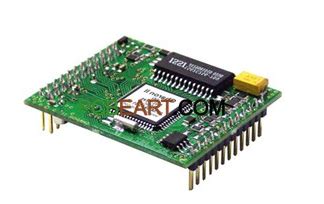
1. Incorrect Component Placement
One of the most common mistakes in PCB assembly is incorrect component placement. This can happen due to human error, incorrect component labeling, or misinterpretation of the assembly drawing.
Corrective Actions
- Double-check the assembly drawing and component labels before placing components
- Use automated component placement machines with vision systems to reduce human error
- Implement a quality control process to verify component placement accuracy
2. Insufficient Solder Paste Application
Applying too little solder paste can result in weak or incomplete solder joints, leading to poor electrical connections and potential product failures.
Corrective Actions
- Use solder paste stencils with the correct aperture size and thickness
- Regularly calibrate and maintain solder paste dispensing equipment
- Monitor solder paste application using automated inspection systems
3. Overheating Components During Soldering
Exposing components to excessive heat during the soldering process can cause damage, leading to reduced performance or complete failure.
Corrective Actions
- Follow the recommended soldering temperature and duration for each component
- Use a controlled heating method, such as a reflow oven with precise temperature profiles
- Minimize the exposure time of components to high temperatures

4. Inadequate Cleaning After Soldering
Failing to properly clean the PCB after soldering can leave flux residue, which can cause corrosion, short circuits, and other issues.
Corrective Actions
- Use an appropriate cleaning solution and method based on the type of flux used
- Ensure complete coverage of the PCB during the cleaning process
- Verify the cleanliness of the PCB using visual inspection or automated inspection systems
5. Incorrect Handling and Storage of PCBs
Improper handling and storage of PCBs can lead to physical damage, contamination, and electrostatic discharge (ESD) events.
Corrective Actions
- Train personnel on proper PCB handling techniques
- Use ESD-safe workstations, tools, and packaging materials
- Store PCBs in a controlled environment with appropriate temperature and humidity levels
6. Insufficient Testing and Quality Control
Skipping or rushing through testing and quality control procedures can allow defects and issues to go undetected, leading to product failures in the field.
Corrective Actions
- Develop and follow a comprehensive testing and quality control plan
- Use automated testing equipment to ensure consistent and accurate results
- Perform both in-circuit and functional testing to catch a wide range of issues
| Mistake | Corrective Actions |
|---|---|
| Incorrect Component Placement | – Double-check assembly drawing and labels – Use automated placement machines – Implement quality control process |
| Insufficient Solder Paste Application | – Use correct solder paste stencils – Calibrate dispensing equipment – Monitor application with inspection systems |
| Overheating Components During Soldering | – Follow recommended soldering temperature and duration – Use controlled heating methods – Minimize exposure time to high temperatures |
| Inadequate Cleaning After Soldering | – Use appropriate cleaning solution and method – Ensure complete PCB coverage – Verify cleanliness with inspection |
| Incorrect Handling and Storage of PCBs | – Train personnel on proper handling techniques – Use ESD-safe workstations and materials – Store PCBs in a controlled environment |
| Insufficient Testing and Quality Control | – Develop and follow comprehensive testing and QC plan – Use automated testing equipment – Perform in-circuit and functional testing |
Frequently Asked Questions (FAQ)
1. What are the most common causes of incorrect component placement?
The most common causes of incorrect component placement include human error, incorrect component labeling, and misinterpretation of the assembly drawing.
2. How can I ensure that the solder paste is applied correctly?
To ensure correct solder paste application, use solder paste stencils with the correct aperture size and thickness, regularly calibrate and maintain solder paste dispensing equipment, and monitor the application process using automated inspection systems.
3. What are the consequences of overheating components during soldering?
Overheating components during soldering can cause damage, leading to reduced performance or complete failure of the component and, consequently, the PCB.
4. Why is it important to clean the PCB after soldering?
Cleaning the PCB after soldering is crucial to remove flux residue, which can cause corrosion, short circuits, and other issues that may affect the performance and reliability of the PCB.
5. What steps can I take to prevent damage to PCBs during handling and storage?
To prevent damage to PCBs during handling and storage, train personnel on proper PCB handling techniques, use ESD-safe workstations, tools, and packaging materials, and store PCBs in a controlled environment with appropriate temperature and humidity levels.
In conclusion, by understanding and addressing these common PCB Assembly Mistakes, you can significantly improve the quality, reliability, and performance of your PCBs. Implementing the corrective actions discussed in this article will help you streamline your assembly process, reduce rework and delays, and ultimately, achieve better results for your products.


Leave a Reply