Introduction to Multilayer PCBs
Multilayer PCBs, also known as multilayer printed circuit boards, are advanced circuit boards that consist of multiple layers of conductive material, separated by insulating layers. These boards are designed to accommodate complex electronic circuits and provide a high degree of functionality in a compact form factor. With the increasing demand for smaller, faster, and more powerful electronic devices, multilayer PCBs have become an essential component in various industries, including telecommunications, aerospace, medical devices, and consumer electronics.
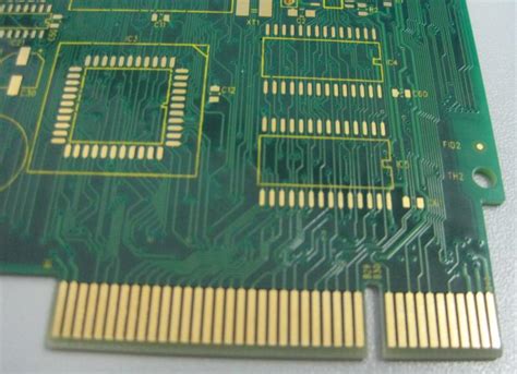
What are 32 Layer PCBs?
32 layer PCBs are a type of multilayer PCB that features 32 layers of conductive material, making them one of the most complex and advanced types of printed circuit boards available. These boards are designed to handle extremely high-density electronic circuits and provide unparalleled performance in terms of signal integrity, power distribution, and thermal management.
Benefits of 32 Layer PCBs
-
High Density: 32 layer PCBs allow for the integration of a large number of components and circuits in a small form factor, enabling the development of compact and powerful electronic devices.
-
Enhanced Signal Integrity: The multiple layers in a 32 layer PCB help to minimize signal interference and crosstalk, ensuring reliable and accurate signal transmission.
-
Improved Power Distribution: The increased number of layers allows for better power distribution, reducing voltage drops and ensuring stable power supply to all components.
-
Efficient Thermal Management: 32 layer PCBs can incorporate dedicated layers for thermal management, helping to dissipate heat generated by components and prevent overheating.
Designing 32 Layer PCBs
Design Considerations
When designing a 32 layer PCB, several key factors must be taken into account to ensure optimal performance and manufacturability:
-
Layer Stackup: The arrangement of conductive and insulating layers is crucial for signal integrity and power distribution. Careful planning of the layer stackup is necessary to minimize signal interference and ensure proper impedance control.
-
Via Placement: Vias are used to interconnect different layers of the PCB. Proper via placement is essential to minimize signal reflections and maintain signal integrity.
-
Component Placement: The placement of components on a 32 layer PCB must be optimized to minimize signal path lengths, reduce crosstalk, and facilitate efficient routing.
-
Routing Strategies: Advanced routing techniques, such as high-speed differential pair routing and controlled impedance routing, are necessary to ensure reliable signal transmission in high-density 32 layer PCBs.
Design Tools and Software
Designing a 32 layer PCB requires the use of advanced PCB Design Tools and software. Some popular options include:
- Altium Designer
- Cadence Allegro
- Mentor Graphics PADS
- Zuken CR-8000
These tools provide powerful features for schematic capture, layout design, signal integrity analysis, and 3D visualization, enabling designers to create complex 32 layer PCBs with ease.

Manufacturing 32 Layer PCBs
Fabrication Process
The fabrication of a 32 layer PCB involves several steps:
-
Inner Layer Fabrication: The inner layers of the PCB are fabricated using a photolithographic process, where the desired circuit pattern is transferred onto a copper-clad laminate.
-
Lamination: The inner layers are stacked and laminated together with insulating material under high pressure and temperature to form a solid board.
-
Drilling: Holes are drilled through the laminated board to accommodate vias and component leads.
-
Plating: The drilled holes are plated with copper to create electrical connections between layers.
-
Outer Layer Fabrication: The outer layers of the PCB are fabricated using a similar photolithographic process as the inner layers.
-
Solder Mask and Silkscreen: A solder mask is applied to protect the copper traces, and a silkscreen is added for component labeling and identification.
Quality Control and Testing
Ensuring the quality and reliability of a 32 layer PCB requires rigorous quality control and testing procedures:
-
Visual Inspection: The fabricated PCB is visually inspected for defects such as scratches, voids, or contamination.
-
Automated Optical Inspection (AOI): An automated optical inspection system is used to detect surface defects and ensure proper component placement.
-
Electrical Testing: Various electrical tests, such as continuity, isolation, and high-potential (HiPot) tests, are performed to verify the electrical integrity of the board.
-
Impedance Testing: Controlled impedance testing is conducted to ensure that the PCB meets the specified impedance requirements for high-speed signals.
-
Microsectioning: In some cases, microsectioning may be performed to examine the internal structure of the PCB and verify the integrity of vias and plated holes.

Applications of 32 Layer PCBs
32 layer PCBs find applications in various industries where high-density, high-performance electronic circuits are required:
Telecommunications
In the telecommunications industry, 32 layer PCBs are used in routers, switches, and base stations to handle high-speed data transmission and complex signal processing.
Aerospace and Defense
Aerospace and defense applications, such as satellites, avionics systems, and radar equipment, rely on 32 layer PCBs for their advanced functionality and reliability in harsh environments.
Medical Devices
Medical devices, such as imaging systems and patient monitoring equipment, utilize 32 layer PCBs to integrate a large number of components and ensure precise signal processing.
High-Performance Computing
32 layer PCBs are essential for high-performance computing applications, such as data centers and supercomputers, where high-speed data transfer and efficient power distribution are critical.

Future Trends in Multilayer PCBs
As electronic devices continue to evolve and become more complex, the demand for advanced multilayer PCBs, such as 32 layer boards, is expected to grow. Some future trends in multilayer PCB technology include:
-
Higher Layer Counts: PCBs with even higher layer counts, such as 48 or 64 layers, may become more common to accommodate the increasing complexity of electronic circuits.
-
Advanced Materials: New materials, such as low-loss dielectrics and high-performance laminates, will be developed to improve signal integrity and thermal management in multilayer PCBs.
-
Embedded Components: The integration of passive components, such as resistors and capacitors, directly into the PCB substrate will become more prevalent to further reduce board size and improve performance.
-
3D Printing: Additive manufacturing techniques, such as 3D printing, may be used to fabricate multilayer PCBs with complex geometries and embedded features.
FAQ
-
What is the difference between a 32 layer PCB and a regular PCB?
A 32 layer PCB has 32 layers of conductive material, while a regular PCB typically has 1-4 layers. The increased number of layers allows for higher density, better signal integrity, and improved power distribution. -
How much does a 32 layer PCB cost compared to a regular PCB?
The cost of a 32 layer PCB is significantly higher than a regular PCB due to the increased complexity of the fabrication process and the advanced materials used. The exact cost difference depends on factors such as board size, quantity, and design complexity. -
What are the design challenges associated with 32 layer PCBs?
Designing a 32 layer PCB requires careful consideration of layer stackup, via placement, component placement, and routing strategies to ensure optimal signal integrity and power distribution. Advanced PCB design tools and expertise are necessary to overcome these challenges. -
How long does it take to manufacture a 32 layer PCB?
The manufacturing lead time for a 32 layer PCB is typically longer than a regular PCB due to the complex fabrication process. Lead times can range from several weeks to a few months, depending on the specific requirements and the manufacturer’s capacity. -
Are 32 layer PCBs suitable for all electronic devices?
While 32 layer PCBs offer numerous benefits, they are not necessary for all electronic devices. The decision to use a 32 layer PCB depends on factors such as the complexity of the circuit, the required performance, and the space constraints of the device. In many cases, PCBs with fewer layers may be sufficient and more cost-effective.
Conclusion
32 layer printed circuit boards represent the pinnacle of multilayer PCB technology, offering unparalleled density, signal integrity, and power distribution for complex electronic circuits. As the demand for smaller, faster, and more powerful electronic devices continues to grow, 32 layer PCBs will play an increasingly important role in various industries, from telecommunications and aerospace to medical devices and high-performance computing.
Designing and manufacturing 32 layer PCBs requires advanced tools, expertise, and rigorous quality control processes to ensure optimal performance and reliability. As technology advances, we can expect to see even more sophisticated multilayer PCBs with higher layer counts, advanced materials, and innovative manufacturing techniques.
By understanding the capabilities, challenges, and applications of 32 layer PCBs, engineers and designers can make informed decisions when developing cutting-edge electronic devices that push the boundaries of performance and functionality.


Leave a Reply