Blog

  • Guide to Create A PCB with KiCad

    Posted by

    Introduction to PCB Design and KiCad Printed Circuit Boards (PCBs) are the backbone of modern electronics. They provide a stable and efficient way to connect electronic components and create complex circuits. Designing a PCB can be a daunting task, especially for beginners. However, with the right tools and guidance, anyone can create a professional-grade PCB.…

    Read more: Guide to Create A PCB with KiCad
  • High Frequency PCB Layout

    Posted by

    Introduction to High Frequency PCB Layout High frequency PCB layout is a crucial aspect of designing printed circuit boards for applications that involve high-speed signals. As the demand for faster data transmission and higher bandwidth increases, designers must pay close attention to the layout of their PCBs to ensure optimal performance and minimize signal integrity…

    Read more: High Frequency PCB Layout
  • Introduction EAGLE (Easily Applicable Graphical Layout Editor) is a powerful PCB Design software that allows users to create professional-grade schematics and PCB Layouts. Whether you’re a hobbyist or a professional engineer, EAGLE provides a user-friendly interface and a comprehensive set of tools to help you bring your electronic designs to life. In this article, we’ll…

    Read more: EAGLE 6 or 7 – Create a project and start drawing the schematic
  • Tolerances on Copper Thickness on a PCB

    Posted by

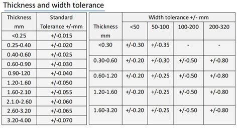
    Understanding Copper Thickness Tolerances in PCB Manufacturing Printed Circuit Boards (PCBs) are the backbone of modern electronics. They provide the electrical connections and mechanical support for various components in electronic devices. One critical aspect of PCB manufacturing is the copper thickness, which plays a vital role in the performance, reliability, and manufacturability of the board.…

    Read more: Tolerances on Copper Thickness on a PCB
  • cEDM – Electronics Design & Manufacturing

    Posted by

    Introduction to cEDM cEDM, which stands for Electronics Design & Manufacturing, refers to the end-to-end process of designing and producing electronic products and components. This encompasses everything from the initial product concept and schematic design, to sourcing components, fabricating printed circuit boards (PCBs), assembling and testing the final product. The cEDM process has evolved significantly…

    Read more: cEDM – Electronics Design & Manufacturing
  • PCBA Visualizer – User Guide – BOM Editor

    Posted by

    Introduction to PCBA Visualizer PCBA Visualizer is a powerful tool that allows users to view and edit PCB designs and their associated Bill of Materials (BOM). It provides a user-friendly interface for navigating complex PCB Layouts and helps streamline the PCB design process. The key features of PCBA Visualizer include: 3D visualization of PCB designs…

    Read more: PCBA Visualizer – User Guide – BOM Editor
  • Welcome to the CadSoft EAGLE V7 Section on Rayming

    Posted by

    Introduction to CadSoft EAGLE V7 CadSoft EAGLE (Easily Applicable Graphical Layout Editor) is a powerful and user-friendly software tool for designing printed circuit boards (PCBs). Developed by CadSoft Computer GmbH, EAGLE has become a popular choice among electronics engineers, hobbyists, and educators due to its versatile features and extensive component libraries. The latest version, CadSoft…

    Read more: Welcome to the CadSoft EAGLE V7 Section on Rayming
  • How to add a couple of solder pads to an Eagle board?

    Posted by

    Understanding solder pads in Eagle Solder pads in Eagle are copper areas on the PCB where components are soldered in place. They provide both electrical connection and mechanical stability for the components. Pads come in various sizes and shapes depending on the component package type (through-hole, surface-mount, etc.). Eagle represents pads as a separate library…

    Read more: How to add a couple of solder pads to an Eagle board?
  • Understanding Bow and Twist on a PCB

    Posted by

    What is PCB Warpage? PCB warpage, also known as PCB bow and twist, is a common issue that occurs during the manufacturing process of printed circuit boards (PCBs). It refers to the distortion or deviation from flatness of the PCB, which can cause various problems in the assembly and functionality of the final product. PCB…

    Read more: Understanding Bow and Twist on a PCB
  • What are PCB Warp & Twist?

    Posted by

    What is PCB Warpage? PCB warpage is the deviation of a printed circuit board from its intended flat shape. It occurs when the board experiences uneven stress or thermal expansion, causing it to bend or twist. The severity of warpage can vary depending on various factors such as material properties, manufacturing processes, and environmental conditions.…

    Read more: What are PCB Warp & Twist?