A filled copper thermal via array under a power pad can reduce board-level thermal resistance by 40–70% compared to bare FR-4, dropping junction temperatures by 15–30 °C in typical QFN and power-pad packages. The key design variables are via diameter, pitch, plating or fill method, and the number of vias that fit under the thermal pad. Get any one of these wrong and you either leave heat on the table or create reliability problems during reflow.
Key Takeaways
- A single 0.3 mm diameter, 1.6 mm deep copper-filled via has a thermal resistance of roughly 45–55 °C/W; an array of 16 drops the combined Rth to about 3–4 °C/W.
- Copper-filled vias outperform plated-only vias by 3–5× in thermal conductivity because solid copper (390 W/mK) replaces the air or solder column inside the barrel.
- Via pitch below 1.0 mm risks barrel-to-barrel shorts and weakens the annular ring; 1.0–1.2 mm center-to-center is the practical minimum for 0.3 mm drill.
- On ceramic substrates with thermal conductivity of 24–170 W/mK, thermal vias are less critical than on FR-4 (0.3 W/mK), but they still matter for multilayer LTCC and thick alumina builds where vertical heat flow is restricted.
- Always cap or fill vias under BGA or QFN pads to prevent solder wicking during reflow, per IPC-7093B guidelines.
What a Thermal Via Actually Does
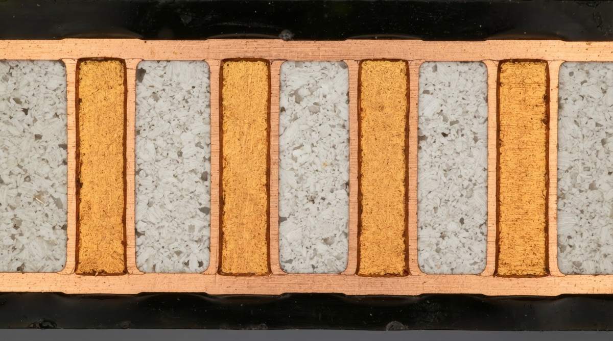
A thermal via is a plated or filled through-hole whose sole purpose is to conduct heat vertically through the board. It connects a surface copper pad—usually the exposed pad of a QFN, BGA, or power MOSFET—to an internal or bottom-side copper plane that acts as a heat spreader. The via itself is a short copper cylinder, and its thermal resistance depends on cross-sectional area, length, and the thermal conductivity of whatever fills the barrel.
In FR-4, the substrate between copper layers conducts heat at only about 0.3 W/mK. A 1.6 mm thick board with no vias under a 5 × 5 mm thermal pad has a substrate Rth of roughly 70–90 °C/W. Adding a 4 × 4 array of copper-filled 0.3 mm vias on 1.2 mm pitch drops that to 3–5 °C/W. The vias become parallel thermal paths that bypass the insulating resin.
Via Geometry and Fill Options
Three parameters define a single via’s thermal performance: diameter, length (board thickness), and fill material.
| Parameter | Typical Range | Unit | Notes |
|---|---|---|---|
| Drill diameter | 0.20–0.40 | mm | 0.30 mm is the most common for thermal vias |
| Plating thickness | 20–35 | µm | Per IPC-6012 Class 2/3 minimum 20 µm |
| Board thickness (via length) | 0.8–2.4 | mm | Shorter = lower Rth |
| Copper fill conductivity | ~390 | W/mK | Electroplated copper fill |
| Solder fill conductivity | ~50 | W/mK | SnAgCu (SAC305) |
| Air (hollow via) conductivity | ~0.026 | W/mK | Effectively insulating core |
| Epoxy fill conductivity | 0.2–0.8 | W/mK | Thermally conductive epoxy up to ~4 W/mK available |
Typical values for commercially available materials, for comparison only. Confirm against the datasheet for your specific grade.
Copper-filled vias offer the best thermal path. The entire barrel is solid copper. Cost is higher because the fab must electroplate the hole shut, then planarize the surface. Solder-filled vias are cheaper but conduct heat at roughly 1/8 the rate of solid copper. Capped vias—plated barrel with a lid of copper over the top—prevent solder wicking but leave an air column that contributes almost nothing thermally. For serious thermal work, copper fill is the right call.
How to Size a Thermal Via Array
Step 1: Determine the Thermal Pad Area
Check the component datasheet for the exposed pad dimensions. A typical QFN-48 has a 5.1 × 5.1 mm thermal pad. A power MOSFET in a DPAK package exposes about 5.2 × 6.1 mm.
Step 2: Choose Via Diameter and Pitch
Use 0.3 mm finished hole diameter with a 0.6 mm pad and 1.0–1.2 mm center-to-center pitch. This keeps the annular ring above the IPC-6012 Class 2 minimum of 50 µm after drill wander and gives enough copper between vias to avoid cracking during thermal cycling.
Step 3: Calculate the Number of Vias
For a 5.1 × 5.1 mm pad on 1.2 mm pitch: floor(5.1 / 1.2) + 1 = 5 vias per side, so a 5 × 5 = 25-via array. On 1.0 mm pitch: 6 × 6 = 36 vias.
Step 4: Estimate Array Thermal Resistance
Each copper-filled via’s Rth is calculated as:
Rth_via = L / (k × A)
Where L is via length (board thickness), k is copper conductivity (390 W/mK), and A is the cross-sectional area of the copper fill (π × r²).
Worked example: 0.3 mm diameter copper-filled via, 1.6 mm board.
- A = π × (0.15 mm)² = 0.0707 mm² = 7.07 × 10⁻⁸ m²
- Rth_via = 0.0016 m / (390 W/mK × 7.07 × 10⁻⁸ m²) = 58 °C/W
For a 25-via array in parallel: Rth_array = 58 / 25 = 2.3 °C/W. Compare that to the ~80 °C/W of bare FR-4 over the same area. The vias reduce vertical thermal resistance by roughly 97%.
Enter your own pad dimensions, via geometry, and board thickness into the calculator below to get an array Rth estimate for your specific layout.
[pcb_calc type=”thermal-via”]
Thermal Vias on Ceramic Substrates
On organic PCBs, thermal vias are essential because FR-4 is a thermal insulator. On ceramic boards the situation is different. A 0.635 mm thick 96% alumina substrate already conducts heat at 24–28 W/mK—roughly 80× better than FR-4. An aluminum nitride substrate reaches 170–200 W/mK. The substrate itself is the heat spreader.
Thermal vias in ceramic are still used in multilayer LTCC builds where internal ground planes or buried components create vertical thermal barriers. In single-layer ceramic, direct metallization on the bottom side often eliminates the need for vias entirely. If you are choosing between adding thermal vias to FR-4 and switching to a ceramic substrate, comparing thermal conductivity across materials will help frame the trade-off.
Common Mistakes in Thermal Via Design

Pitch too tight. Vias on 0.6 mm pitch with 0.3 mm drill leave only 0.15 mm of laminate between barrels. This cracks during thermal cycling (–40 to +125 °C, per IPC-TM-650 2.6.7.2) and can cause internal shorts. Keep pitch ≥ 1.0 mm unless your fab explicitly supports tighter rules.
Unfilled vias under BGA pads. Open vias wick solder away from the joint during reflow, creating voids and weak connections. IPC-7093B recommends via-in-pad be filled and planarized for any pad that receives a solder ball.
Ignoring the bottom-side plane. Vias dump heat downward. If there is no copper plane or heatsink on the bottom to spread and convect that heat, the via array’s benefit is wasted. Always pair thermal vias with a bottom copper pour connected to a heatsink or chassis. For board-level strategies, see the guide on ceramic heat spreader design.
Over-counting the improvement. The via array’s Rth is only one link in the thermal chain. Junction-to-case, TIM, and heatsink-to-ambient resistances usually dominate. Running a thermal resistance calculation for the full stack is the only way to know whether the via array is the bottleneck.
When Thermal Vias Are Not the Right Solution
If your board is a single-layer ceramic substrate (alumina or AlN) with direct copper bonding on both sides, the substrate’s own conductivity handles vertical heat flow. Adding vias to a 0.635 mm alumina board gains almost nothing because the ceramic is already 80× more conductive than FR-4.
For very high power densities (above ~200 W/cm²), even copper-filled vias in FR-4 cannot keep junction temperatures safe. At that point, you need a direct-bonded copper (DBC) or active metal brazed (AMB) ceramic substrate, or a metal-core board. Thermal vias are a workaround for low-conductivity substrates; they are not a substitute for choosing the right base material.
If your design dissipates under 0.5 W and operates within commercial temperature range (0–70 °C), standard FR-4 with a modest ground pour is usually sufficient. Adding thermal vias would increase cost without meaningful benefit.
Frequently Asked Questions
Do thermal vias need to be filled with copper?
Copper fill gives the best thermal result—roughly 5× lower Rth than a plated-only via with an air core. However, solder-filled or epoxy-filled vias are acceptable when the power dissipation is moderate (under 1–2 W per component). Copper fill costs more and requires a fab capable of via-fill-and-planarize processing.
How close can I place thermal vias to signal vias?
Maintain at least 0.5 mm edge-to-edge clearance between a thermal via barrel and any signal via or trace. Tighter spacing risks drill breakout and crosstalk. Your fab’s design rule check (DRC) file will enforce the minimum they support.
Can I put thermal vias inside a BGA pad?
Yes, but only if the vias are filled and planarized flush with the pad surface. Open or tented vias under BGA balls cause solder voids that degrade both thermal and electrical connections. IPC-7093B Section 5.3 covers via-in-pad requirements for BGA assemblies.
Do thermal vias help on a metal-core PCB?
Minimally. A metal-core PCB already has an aluminum or copper base layer with conductivity of 150–390 W/mK. The dielectric layer (typically 75–150 µm thick) is the thermal bottleneck, and vias do not pass through it. Improving the dielectric material or reducing its thickness is more effective on MCPCBs.
How many thermal vias do I need under a QFN?
A 4 × 4 or 5 × 5 array on 1.0–1.2 mm pitch is standard for a 5 mm × 5 mm exposed pad. More vias reduce Rth further, but returns diminish beyond about 25 vias because the bottom copper plane’s spreading resistance becomes the new bottleneck.
Next Step
If your thermal analysis shows that FR-4 with vias still cannot meet your junction temperature target, it may be time to evaluate a ceramic substrate. Read the ceramic PCB thermal management guide for a direct comparison of substrate options. Ready to get pricing on a ceramic board for your thermal design? Request a quote from AluminaPCB.