Ceramic PCB singulation requires methods matched to the hardness and brittleness of the substrate. Standard FR-4 depaneling tools—pizza cutters, hook-blade routers, punch dies—will crack or shatter alumina and aluminum nitride. The four proven ceramic singulation methods are laser cutting, scribe-and-break, diamond-wheel sawing, and pre-routed breakaway tabs. Each method trades off edge quality, dimensional tolerance, throughput, and cost differently.
Key Takeaways
- Laser cutting delivers the tightest singulation tolerance on ceramics, typically ±25–50 µm, with no mechanical stress on the substrate.
- Scribe-and-break is the lowest-cost method for straight-line separation of Al₂O₃ panels, but it cannot produce curved outlines.
- Diamond-wheel sawing suits thick substrates (≥0.5 mm) and achieves ±50–100 µm tolerance, though it generates kerf waste and requires coolant.
- Pre-routed breakaway tabs let you depanel after assembly, but tab design must account for ceramic’s zero ductility.
- Edge chipping is the dominant failure mode in all mechanical singulation methods; laser cutting largely eliminates it.
Why Ceramic Singulation Differs from FR-4 Depaneling
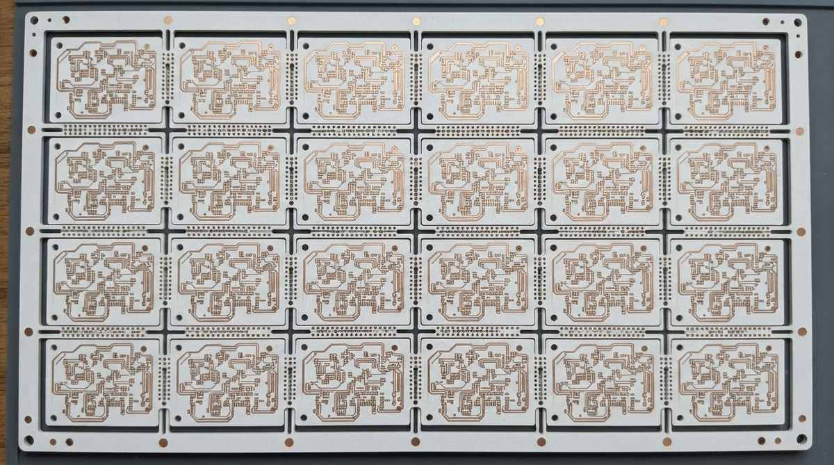
FR-4 is a glass-epoxy laminate with some flex. Ceramic substrates—Al₂O₃, AlN, Si₃N₄—are fully sintered oxide or nitride bodies with zero plastic deformation. A force that would bend an FR-4 panel simply fractures a ceramic one. This means every singulation method must either cut through the material (laser, saw) or guide a fracture along a pre-defined path (scribe-and-break, breakaway tabs).
Metallization adds another constraint. Ceramic metallization layers—whether DPC copper, thick film silver, or thin film gold—can delaminate at a cut edge if the process introduces excessive thermal shock or vibration. Method selection must consider both the bare substrate and whatever conductor stack sits on top of it.
Laser Cutting
CO₂ and UV (Nd:YAG, 355 nm) lasers are the most common sources for ceramic singulation. CO₂ lasers work well for Al₂O₃ up to about 1.0 mm thick; UV lasers are preferred for AlN and for thinner substrates where the heat-affected zone (HAZ) must be minimized.
Laser cutting is a non-contact process. There is no mechanical load on the substrate, so edge chipping is essentially zero. The kerf is narrow—typically 30–80 µm depending on beam diameter and material thickness. Positional accuracy of ±25–50 µm is achievable on modern galvo-scan systems.
The main drawback is speed. Cutting through 0.635 mm Al₂O₃ at production rates may require multiple passes, reducing throughput compared to scribe-and-break. Cost per unit is higher for simple rectangular outlines but competitive or lower for complex shapes, because laser paths cost the same regardless of geometry. Laser systems also handle laser drilling of vias and singulation on the same machine in some workflows, consolidating process steps.
Worked Example: Laser Singulation of a 50 × 50 mm Unit
Assume a 150 × 100 mm Al₂O₃ 96% panel, 0.635 mm thick, containing six 50 × 50 mm units. Total cut length per panel: approximately 700 mm (perimeter cuts plus internal streets). At a CO₂ laser feed rate of ~15 mm/s with two passes, cut time is roughly 95 seconds per panel, or about 16 s per unit. Adding load/unload, throughput is approximately 150–180 units per hour on a single machine.
Scribe-and-Break
A diamond-tipped scribe (or laser scribe) scores a groove on one or both sides of the ceramic panel along the desired break line. The groove depth is typically 25–35 % of substrate thickness. The panel is then broken along the scribe by applying a three-point bending force.
This method is fast and inexpensive. It works best for straight-line cuts on Al₂O₃ panels up to about 1.0 mm thick. Edge roughness is moderate—fracture surfaces show the grain structure of the ceramic, with Ra values around 1–3 µm. Dimensional tolerance is ±75–150 µm, wider than laser, because the fracture path can deviate slightly from the scribe line.
Scribe-and-break cannot produce curved outlines, internal cutouts, or L-shaped boards. It is also risky on AlN, which has a different fracture behavior and tends to propagate cracks away from the scribe line more readily than alumina. For panels with fine-pitch metallization near the break edge, the mechanical shock of snapping can cause micro-cracks that propagate into conductor pads.
Diamond-Wheel Sawing
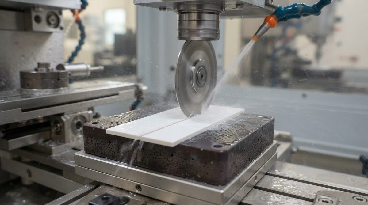
A resin-bonded or nickel-bonded diamond blade spins at high RPM and cuts through the ceramic with coolant (usually deionized water). This is the same principle as semiconductor wafer dicing, scaled up for larger substrates.
Sawing handles any substrate thickness and both straight and moderately curved cuts. Kerf width is 150–300 µm depending on blade thickness, which means more material waste per street than laser. Tolerance is ±50–100 µm. Edge chipping on the exit side of the blade is the primary quality concern; it can be reduced with slower feed rates, finer grit blades, and cutting from both sides.
Coolant management matters. Residual water and slurry must be cleaned from the panel after cutting, especially if the board carries wire-bondable metallization. Any contamination on copper-plated surfaces or gold pads degrades bond quality.
Pre-Routed Breakaway Tabs (Mouse Bites)
Breakaway tabs let you process an entire panel through SMT assembly and then singulate individual units at the end of the line. The panel is manufactured with routed slots between units, leaving small connecting tabs—often perforated with a row of small holes (mouse bites) to control the break force.
Designing breakaway tabs for ceramic demands caution. Unlike FR-4, where a tab can flex before snapping, a ceramic tab transmits the break force directly. If the tab is too wide, the break force cracks the unit. If it is too narrow, the tab fractures during handling before assembly. A typical starting point for 0.635 mm Al₂O₃ is a tab width of 0.8–1.2 mm with 3–5 drilled perforations of 0.3 mm diameter spaced 0.5 mm apart.
Enter your substrate thickness, unit dimensions, and number of tabs to estimate recommended tab width and perforation layout for ceramic breakaway panels.
[pcb_calc type=”breakaway-tab”]
After break, the tab remnant (nub) must be ground or lapped flush if the edge is functional. Lapping and grinding services can bring the nub to within ±25 µm of the nominal edge, but this adds cost and cycle time.
Comparison of Ceramic Singulation Methods
| Parameter | Laser Cutting | Scribe-and-Break | Diamond Saw | Breakaway Tabs |
|---|---|---|---|---|
| Dimensional tolerance | ±25–50 µm | ±75–150 µm | ±50–100 µm | ±100–200 µm (as-broken) |
| Edge chipping risk | Very low | Low–moderate | Moderate | Moderate–high at nub |
| Outline geometry | Any (curves, cutouts) | Straight lines only | Straight + gentle curves | Any (routed pre-fire or laser-cut) |
| Max practical thickness | ~1.0 mm (CO₂), ~0.5 mm (UV) | ~1.0 mm | No practical limit | ~1.0 mm |
| Kerf width | 30–80 µm | ~0 (fracture) | 150–300 µm | N/A (pre-routed slot) |
| Throughput (relative) | Medium | High | Medium–low | High (break is fast) |
| Relative cost per unit | Medium–high | Low | Medium | Low (if no post-processing) |
| Suitable for post-assembly depaneling | Yes (with fixturing) | No (stresses components) | Yes (with coolant control) | Yes (primary use case) |
Typical values for commercially available processes, for comparison only. Actual results depend on substrate material, thickness, metallization, and equipment.
When Not to Use Each Method
Laser cutting is overkill for simple rectangular units on thin Al₂O₃ where scribe-and-break meets your tolerance. The cost premium is hard to justify if edge quality is non-critical.
Scribe-and-break should be avoided for AlN substrates, curved outlines, or any board where metallization runs within 0.3 mm of the break edge. The fracture path is not perfectly controllable.
Diamond sawing is a poor choice for substrates thinner than 0.25 mm—blade vibration causes excessive chipping. It also requires thorough post-cut cleaning, which adds time and cost if you have wire-bond pads.
Breakaway tabs are not suitable when post-break edge quality must be better than ±100 µm without secondary grinding, or when the substrate is too thin (below ~0.38 mm) to support a stable tab.
If your board is a standard rectangle on FR-4 or metal-core laminate, conventional V-score or routing depaneling is cheaper and faster than any ceramic method. Ceramic singulation costs are justified only when the substrate itself must be ceramic for thermal, dielectric, or high-temperature reasons.
Design Tips for Clean Singulation
- Keep copper traces and pads at least 0.3 mm from the singulation edge (0.5 mm preferred) to avoid delamination and chipping into conductors.
- Specify the singulation method on your fab drawing. The panel layout, street width, and fiducial placement all change depending on the method.
- For laser-cut boards, mark the cut side and any critical datum edges. Laser marking for part identification can be done in the same setup as singulation on some systems.
- If using scribe-and-break, orient scribe lines parallel to the substrate’s firing direction when known—crack propagation is more predictable along the grain.
- For breakaway tabs, place tabs away from corners. Corner tabs concentrate stress and increase the risk of diagonal cracks into the unit.
Frequently Asked Questions
Can I use a standard PCB router to depanel ceramic boards?
No. Standard carbide routing bits are not hard enough to cut sintered alumina or AlN and will shatter the substrate. Diamond-coated or diamond-grit tools are required for any mechanical cutting of ceramic PCBs.
Does laser singulation damage copper traces near the cut edge?
Copper reflects CO₂ laser wavelengths efficiently, so traces are not directly ablated. However, the heat-affected zone extends roughly 50–100 µm from the kerf. Keeping traces at least 0.3 mm from the cut line avoids thermal damage to adhesion layers.
What street width should I leave between units for diamond sawing?
Allow at least the blade kerf (150–300 µm) plus 0.2 mm on each side for chipping and alignment. A 0.8–1.0 mm street is a safe starting point for a 200 µm blade on 0.635 mm Al₂O₃.
Is scribe-and-break reliable for AlN substrates?
It is less reliable than for Al₂O₃. AlN’s thermal conductivity and crystal structure cause cracks to propagate less predictably. Laser scribing improves the result versus mechanical scribing, but laser cutting or sawing is generally preferred for AlN singulation.
Can I singulate ceramic panels after SMT assembly?
Yes, using laser cutting, diamond sawing, or breakaway tabs. Scribe-and-break is not recommended post-assembly because the bending force can crack solder joints or damage components near the break line.
Next Step
If you are designing a panelized ceramic PCB and need to choose a singulation method, send your panel layout and unit dimensions for a review. Our process engineers can recommend the method that balances your edge-quality spec, throughput, and budget. Request a quote with your Gerber files and singulation requirements.