Silicon carbide power modules need ceramic substrates that survive continuous operation at 175–200 °C, match SiC’s coefficient of thermal expansion (CTE) of roughly 4.0 ppm/°C, and conduct enough heat to keep junction temperatures within safe limits. The right ceramic PCB design for a SiC power module combines an aluminum nitride (AlN) or silicon nitride (Si₃N₄) substrate with a direct-bonded copper (DBC) or active metal brazing (AMB) metallization, carefully sized traces, and a layout that minimizes thermal resistance from die to heatsink.
Key Takeaways
- AlN substrates (170–200 W/m·K) offer the lowest thermal resistance path, while Si₃N₄ substrates (70–90 W/m·K) provide roughly 3× the flexural strength for improved power-cycling reliability.
- AMB on Si₃N₄ tolerates more than 10× the power cycles of DBC on Al₂O₃ at ΔT = 100 K, per Infineon and Danfoss published reliability data.
- CTE mismatch between substrate and SiC die should stay below 2 ppm/°C to avoid solder-joint fatigue over thermal cycling from −40 °C to 200 °C.
- Copper thickness of 0.3 mm on DBC or AMB is typical for SiC modules carrying 100–300 A; thicker copper lowers Rth but increases residual stress after bonding.
Why Ceramic PCB Design Matters for SiC Power Modules
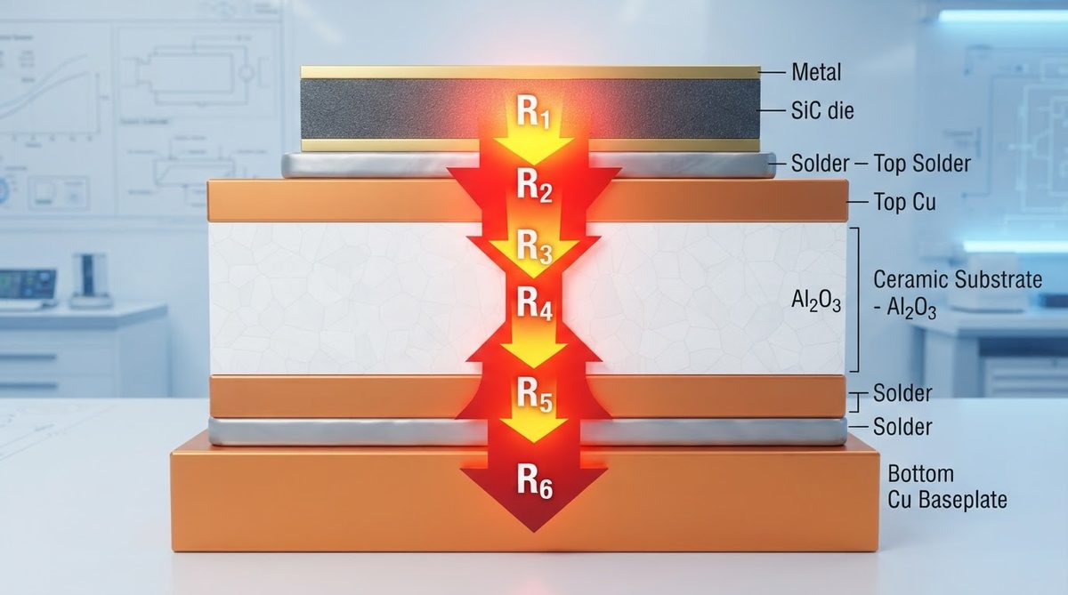
SiC MOSFETs and diodes operate at junction temperatures of 175 °C and above—well past the glass transition temperature of FR-4 (130–140 °C) and the continuous rating of most metal-core PCBs. A ceramic substrate stays dimensionally stable and electrically insulating at these temperatures. Alumina (Al₂O₃), AlN, and Si₃N₄ all have no glass transition; their properties degrade only gradually above 800 °C.
Beyond temperature, CTE matching matters. SiC die have a CTE of approximately 4.0 ppm/°C (per Wolfspeed C3M datasheet). AlN sits at 4.5–5.0 ppm/°C, and Si₃N₄ at 2.5–3.5 ppm/°C. Both are far closer to SiC than alumina (6.5–7.0 ppm/°C) or copper (17 ppm/°C). A smaller CTE gap reduces shear stress in the die-attach solder layer during thermal cycling, directly extending module lifetime. Refer to the ceramic PCB design guidelines for general DFM rules that apply across all ceramic substrates.
Substrate Material Comparison for SiC Modules
| Parameter | Al₂O₃ 96% | AlN | Si₃N₄ | Unit | Condition |
|---|---|---|---|---|---|
| Thermal conductivity | 24–28 | 170–200 | 70–90 | W/m·K | 20 °C, ASTM E1461 |
| CTE | 6.5–7.0 | 4.5–5.0 | 2.5–3.5 | ppm/°C | 20–300 °C |
| Flexural strength | 300–380 | 300–400 | 600–900 | MPa | ASTM C1161, 3-pt bend |
| Dielectric strength | 10–15 | 14–17 | 12–18 | kV/mm | IEC 60672 |
| Max continuous use temp. | ~1000 | ~800 (oxidation limit in air) | ~1000 | °C | Manufacturer guidance |
Typical values for commercially available material, for comparison only. Confirm against the datasheet for your specific grade. Sources: Kyocera SN series datasheet; Maruwa AlN datasheet; CoorsTek AD-96 datasheet.
For most SiC power modules, the ceramic PCB design choice comes down to AlN vs. Si₃N₄. AlN wins on raw thermal performance; Si₃N₄ wins on mechanical toughness and power-cycling endurance. If your module sees fewer than 50,000 power cycles at ΔT > 80 K, AlN with DBC is cost-effective. For automotive traction inverters requiring millions of cycles, Si₃N₄ with AMB is the safer bet. Design considerations for EV and traction power modules expand on this trade-off.
DBC vs. AMB: Choosing the Copper Bonding Method
DBC (direct bonded copper) uses a copper–oxide eutectic at ~1065 °C to bond copper foil to the ceramic. It works well on Al₂O₃ and AlN, is widely available, and supports copper thicknesses of 0.2–0.5 mm. The bond interface is the weak point under thermal cycling: micro-cracks propagate at the copper–ceramic boundary after repeated ΔT excursions.
AMB (active metal brazing) uses a Ti- or Zr-containing braze alloy at ~850 °C. The braze chemically wets the ceramic, producing a stronger interface. AMB is the standard process for Si₃N₄ substrates because DBC does not bond reliably to Si₃N₄. AMB also allows thicker copper (up to 0.8 mm) and tighter pattern resolution than DBC.
For SiC modules operating above 175 °C with aggressive thermal cycling, AMB on Si₃N₄ provides the longest service life. Published data from Danfoss Bond Buffer studies show AMB/Si₃N₄ substrates surviving >100,000 power cycles at ΔT = 150 K, compared to <10,000 cycles for DBC/Al₂O₃ under the same conditions. The bonding method is a critical decision in any ceramic PCB design for a SiC power module, and it should be locked down before layout begins.
Thermal Layout: A Worked Example
Consider a half-bridge SiC module with two 10 mm × 10 mm MOSFET die, each dissipating 150 W at rated load. The substrate is 0.635 mm thick AlN with 0.3 mm DBC copper on both sides.
Step 1 — Substrate thermal resistance:
Rth,substrate = t / (k × A) = 0.000635 m / (180 W/m·K × 0.0001 m²) = 0.035 °C/W per die.
Step 2 — Copper spreading resistance (top copper):
The 0.3 mm copper layer spreads heat beyond the die footprint. Using a spreading resistance approximation for a 10 mm die on a 20 mm × 20 mm copper pad: Rth,Cu ≈ 0.02 °C/W.
Step 3 — Solder layers:
Die-attach (SAC305, 50 µm thick, k ≈ 60 W/m·K): Rth,solder1 = 0.00005 / (60 × 0.0001) = 0.008 °C/W. Baseplate solder (100 µm): Rth,solder2 ≈ 0.017 °C/W.
Step 4 — Total die-to-heatsink:
Rth,total ≈ 0.008 + 0.02 + 0.035 + 0.017 = 0.08 °C/W. At 150 W, ΔT = 12 °C from die to heatsink surface. With a heatsink at 80 °C, junction temperature reaches approximately 92 °C—well within the 175 °C limit, leaving margin for transient overloads.
If you replaced the AlN substrate with 96% Al₂O₃ (k = 25 W/m·K), Rth,substrate jumps to 0.254 °C/W, and junction temperature rises to roughly 125 °C under the same conditions. That eliminates most of your thermal margin.
Enter your substrate material, thickness, die area, and dissipated power below to estimate junction-to-heatsink thermal resistance for your own ceramic PCB design SiC power module stack-up.
Design Rules Specific to SiC Ceramic Substrates
Minimum Clearances at High Voltage
SiC modules often switch 800–1700 V. Per IPC-2221B and IEC 60664-1, creepage and clearance on ceramic at these voltages require careful pad spacing. On an uncoated ceramic surface with a comparative tracking index (CTI) above 600 V (typical for AlN and Si₃N₄), minimum creepage for 1200 V working voltage is approximately 6.3 mm per IEC 60664-1 at pollution degree 2. Consult your ceramic PCB manufacturing process documentation for achievable minimums on specific substrate sizes.
Copper Pattern and Symmetry
Always balance copper area on top and bottom of the substrate. Asymmetric copper causes bowing during cool-down from the bonding temperature. A general rule: keep the copper area ratio between top and bottom within 80–100%. If the bottom is a full ground plane, the top pattern should cover at least 80% of the same area.
Die-Attach Pad Finish
For SiC die attach using sintered silver (the preferred high-temperature join), the copper pad needs a thin Ni/Au or Ni/Ag plating. Bare copper oxidizes during the sintering process (230–280 °C, 20–30 MPa), creating voids that increase thermal resistance. Typical plating: 3–6 µm electroless Ni + 0.05–0.1 µm immersion Au. Review surface finish options for ceramic substrates to match the finish to your die-attach process.
When Not to Use a Ceramic Substrate for SiC
Ceramic is not always the right answer. If your SiC device operates below 150 W total dissipation in a benign thermal environment (ambient < 50 °C, no aggressive cycling), an insulated metal substrate (IMS) or thick-copper FR-4 may be adequate at a fraction of the cost. Ceramic substrates also add complexity in mechanical assembly—they are brittle and cannot be drilled or routed after metallization without specialized laser processing. For low-voltage SiC applications (<600 V) with modest current, standard IGBT substrate design approaches on Al₂O₃ DBC may be more cost-effective than AlN or Si₃N₄ AMB.
If your module is a prototype with fewer than 50 units, the NRE for AMB tooling may not be justified. In that case, standard DBC on AlN substrates with existing panel sizes can reduce upfront cost. Understanding ceramic PCB cost drivers helps you make this call early in the project.
FAQ
Can I use alumina instead of AlN for a SiC power module?
Yes, but with significant thermal penalty. Al₂O₃ 96% conducts heat at 24–28 W/m·K versus 170–200 W/m·K for AlN. For SiC die dissipating more than about 50 W each, the higher substrate thermal resistance raises junction temperature into unsafe territory. Alumina also has a larger CTE mismatch with SiC (6.5–7.0 vs. 4.0 ppm/°C), reducing solder-joint reliability under thermal cycling.
What copper thickness should I specify for a 200 A SiC module?
Most 200 A SiC half-bridge modules use 0.3 mm DBC or AMB copper. This thickness carries the current with acceptable resistive losses (sheet resistance ~0.19 mΩ/sq at 0.3 mm) while keeping residual stress manageable. Going to 0.5 mm improves current handling but increases the risk of ceramic cracking during thermal cycling, especially on AlN.
Is sintered silver necessary for SiC die attach on ceramic?
Sintered silver is preferred for SiC because it remains stable above 200 °C, unlike SAC305 solder which approaches its melting point at 217 °C. For modules rated at 175 °C junction temperature or above, sintered silver (or sintered copper, in newer processes) is effectively required for long-term reliability. Below 150 °C junction, high-lead solder (Pb93.5Sn5Ag1.5, liquidus 296 °C) is an alternative.
How do I prevent ceramic substrate cracking during assembly?
Cracking usually results from asymmetric copper patterns, excessive screw torque during module assembly, or CTE mismatch with the baseplate. Balance copper on both substrate faces, use compliant thermal interface material between substrate and baseplate, and torque fasteners to the module manufacturer’s specification—typically 0.3–0.5 N·m for M3 screws on ceramic-based modules.
What is the typical cost difference between DBC/AlN and AMB/Si₃N₄?
AMB on Si₃N₄ costs roughly 2–4× more per substrate than DBC on AlN, depending on volume and pattern complexity. The premium buys significantly better power-cycling life. For automotive traction inverters where warranty requirements demand millions of thermal cycles, the added cost is justified. For industrial drives with moderate cycling, DBC/AlN is usually sufficient.
Next Step
If you are specifying a ceramic PCB design for a SiC power module, start by defining your die count, total dissipation, operating voltage, and required power-cycling life. Review the complete ceramic PCB design guide for layout and DFM rules, then request a quote with your substrate dimensions and copper requirements.