Thin film ceramic PCBs typically cost $35–$150+ per 1″×1″ panel in production volumes, roughly 2–5× the price of an equivalent thick film ceramic board. The premium comes from vacuum deposition equipment, tighter tolerances (line/space down to 10–25 µm), and lower throughput per run. Whether that premium is justified depends on your frequency, density, and tolerance requirements.
Key Takeaways
- Expect $35–$150+ per small panel at volumes of 100–500 pieces; unit cost drops 30–50% at 1,000+ pieces.
- Sputtering and photolithography account for 40–60% of total fabrication cost.
- Substrate material matters: 96% Al₂O₃ is the cheapest base; AlN adds 3–5× to substrate cost alone.
- Thin film is cost-effective only when you need line/space below 50 µm, resistor tolerances under ±1%, or frequencies above 10 GHz.
- For features wider than 75 µm and tolerances above ±5%, thick film ceramic delivers comparable performance at lower cost.
What Makes Thin Film Ceramic More Expensive Than Thick Film?
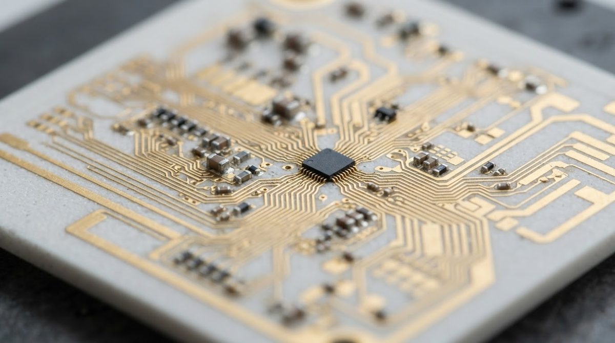
Thin film processing uses vacuum deposition (sputtering or evaporation) followed by photolithographic patterning and wet or dry etching. Each of those steps requires capital-intensive equipment, cleanroom conditions, and skilled operators. Thick film, by contrast, uses screen printing and furnace firing—processes with higher throughput and lower equipment cost per unit.
The practical result: a thick film ceramic circuit with 100 µm lines on 96% alumina might cost $12–$40 per panel in the same quantity where a thin film version with 25 µm lines costs $50–$120. The gap narrows at high volume because sputtering tools run continuously, but it never fully closes.
Thin Film Ceramic Cost Breakdown by Process Step
| Process Step | Share of Total Cost | Key Variables |
|---|---|---|
| Substrate (polished ceramic) | 15–25% | Material grade, surface finish (Ra < 0.05 µm typical for thin film) |
| Metal deposition (sputtering) | 20–30% | Number of target materials (Ti/Pt/Au, TiW/Au, NiCr/Au), layer count |
| Photolithography & etching | 20–30% | Minimum feature size, number of mask layers, alignment tolerance |
| Thin film resistor trimming | 5–15% | Tolerance target (±1% vs ±0.1%), quantity of resistors per panel |
| Surface finish & singulation | 5–10% | Gold thickness, laser vs diamond scribe singulation |
| Test & inspection | 5–10% | RF probe testing, visual inspection criteria |
Typical cost distribution for a single-metal-layer thin film circuit on 96% Al₂O₃. Actual shares vary by design complexity.
The substrate itself deserves attention. Thin film demands a polished surface—typically Ra below 0.05 µm per ASTM B946—because sputtered films are only 0.1–2 µm thick and replicate every surface defect. Polished 96% alumina substrates cost roughly $3–$8 per 1″×1″ piece. Polished AlN substrates run $15–$40 for the same size, per pricing from suppliers like Maruwa and Kyocera.
Worked Example: Budgeting a 10 GHz Filter on Thin Film Alumina
Suppose you need a 25 mm × 25 mm bandpass filter on 96% Al₂O₃ with 20 µm line/space, a single TiW/Au metal layer (0.5 µm Au), and no embedded resistors.
- Substrate (polished): ~$5 per piece
- Sputtering (TiW adhesion + Au seed): ~$18 per piece at 200-piece batch
- Photolithography + etch (one mask layer): ~$15 per piece
- Au plating to 0.5 µm: ~$8 per piece
- Singulation + inspection: ~$6 per piece
- Estimated total: ~$52 per piece at 200 units
At 1,000 units, sputtering and litho costs per piece drop roughly 35%, bringing the unit closer to $35. At prototype quantities of 5–10 pieces, expect $120–$180 each because NRE for the photomask ($300–$800) and machine setup are amortized over very few units. For more detail on prototype pricing, see the ceramic PCB prototype cost guide.
Thin Film vs. Thick Film: When Is the Extra Cost Justified?
| Parameter | Thin Film | Thick Film | Cost Impact |
|---|---|---|---|
| Minimum line/space | 10–25 µm | 75–125 µm | Thin film 2–5× more |
| Resistor tolerance | ±0.1% (laser trimmed) | ±1–5% | Trimming adds 5–15% to thin film cost |
| Conductor thickness | 0.1–3 µm | 8–15 µm | Thin film uses less metal but more process steps |
| Surface roughness (Ra) | < 0.05 µm | 0.3–1.0 µm | Polished substrates cost 2–3× more |
| Frequency sweet spot | > 10 GHz | < 6 GHz | Thin film pays for itself in RF performance above 10 GHz |
| Typical unit cost (1″×1″, qty 500) | $40–$90 | $12–$35 | — |
Values are representative ranges for single-layer circuits on 96% Al₂O₃. Multi-layer or AlN designs shift both columns upward.
If your design needs 100 µm traces at ±5% resistor tolerance for a sensor heater, thick film wins on cost and lead time. If you are building a Ka-band (26–40 GHz) hybrid module where conductor edge definition directly affects insertion loss, thin film is the only practical option. The cost difference becomes irrelevant when the alternative is a board that fails RF spec. For a full breakdown of all ceramic process costs, see the ceramic PCB cost overview.
How to Reduce Thin Film Ceramic Cost
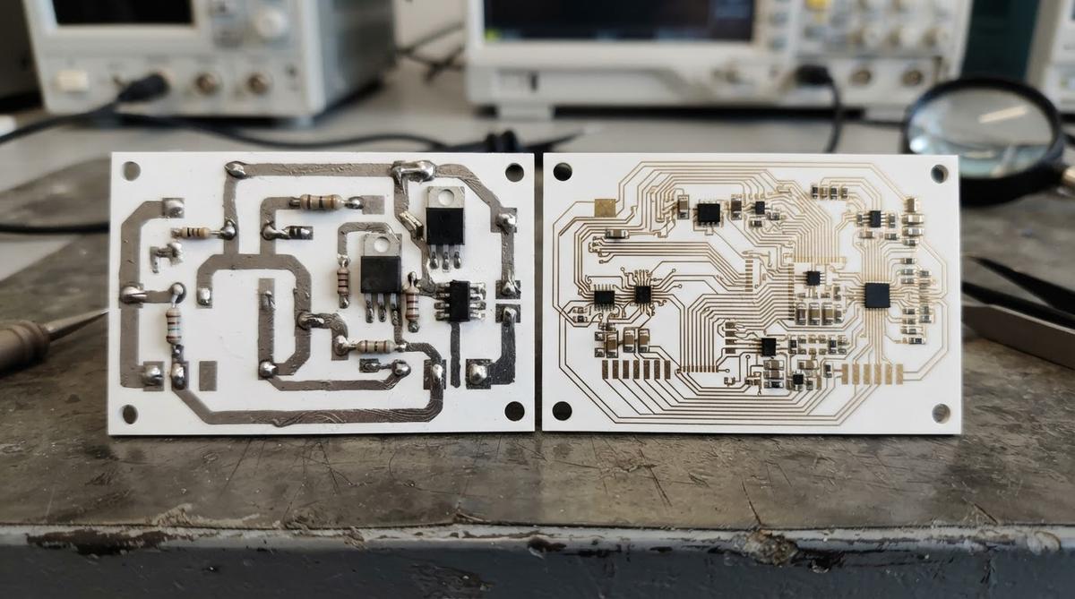
Panelize aggressively. Sputtering and lithography costs scale with machine time, not panel count. Fitting 20 circuits on a 4″×4″ substrate instead of processing them individually can cut per-unit cost by 40–60%.
Minimize mask layers. Each photomask adds $300–$800 NRE and one litho pass. Combining ground planes and signal traces on one layer where electrically feasible removes an entire process cycle.
Relax tolerances where possible. Moving from ±0.1% to ±1% on thin film resistors can eliminate the laser trim step entirely, saving 5–15% of unit cost.
Choose 96% alumina over AlN unless thermal performance demands it. Substrate cost alone drops 3–5× when you stay on Al₂O₃. For strategies that apply across all ceramic processes, the guide on reducing ceramic PCB cost covers additional approaches.
When Not to Use Thin Film Ceramic
Thin film is the wrong choice when your design does not require its defining advantages. Specifically:
- Features above 75 µm: Thick film or DPC achieves this at a fraction of the cost.
- High current paths needing > 5 µm copper: Thin film conductors are too thin. DBC or AMB is more appropriate.
- Cost-sensitive, high-volume consumer products: Standard FR-4 or metal-core PCBs will almost always be cheaper and sufficient.
- Prototypes where you are still iterating the layout: Each mask revision costs $300–$800 and days of lead time. Consider thick film for early iterations, then move to thin film for final production.
Frequently Asked Questions
How much does a thin film ceramic prototype cost?
A single prototype panel typically costs $120–$250, with photomask NRE of $300–$800 on top. Most of the expense is setup and machine time, not materials. Ordering 5–10 prototypes in the same run drops the per-unit cost substantially.
Is thin film ceramic cheaper at high volume?
Yes. Unit cost can drop 50–65% from prototype to 5,000-piece production because sputtering, lithography, and inspection steps run continuously with minimal per-piece overhead. The crossover where thin film becomes cost-competitive with alternative technologies depends on feature size requirements.
Does substrate material affect thin film cost more than process choice?
Substrate material is the second-largest cost driver after sputtering. Switching from 96% Al₂O₃ to AlN increases substrate cost 3–5× and may require adjusted sputter recipes, adding process development charges on first runs.
Can I mix thin film and thick film on the same ceramic substrate?
Yes, hybrid designs are common. Thin film is used for precision resistors or fine-pitch RF traces, while thick film handles power routing or lower-tolerance components on the same substrate. This approach limits thin film processing to only the layers that need it, reducing overall cost.
What is the typical lead time for thin film ceramic boards?
Production lead times run 4–8 weeks depending on complexity and substrate availability. Prototypes can sometimes ship in 2–3 weeks if photomask blanks and substrates are in stock. Rush services are available from some fabricators at a 25–50% premium.
Next Step
If you have a thin film design ready for quoting, or want to compare thin film against LTCC or co-fired alternatives, request a quote with your Gerber files and target quantity. Pricing varies enough by feature size and volume that a project-specific estimate is the only reliable number.