Ceramic PCB Manufacturer

Ceramic substrates that move heat where copper can't.

Custom alumina, aluminum nitride and silicon nitride PCBs — engineered for power modules, EV inverters, high-power LED and RF. From prototype to volume, with DBC, AMB, DPC and thin-film metallization.

170+
W/mK thermal conductivity (AlN)
±10µm
Thin-film line accuracy
72h
Rapid prototype turnaround
Built to qualified standards
ISO 9001 IATF 16949 UL Listed RoHS / REACH ISO 13485
Ceramic Material

Pick the substrate by the physics, not the price list.

Each ceramic trades thermal conductivity, mechanical strength and cost differently. Here's how the four we manufacture compare — and where each one wins.

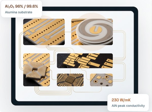
Alumina (Al₂O₃) 96% / 99.6% purity

The industry workhorse. Cost-effective, mechanically stable and dependable for the majority of power and LED designs.

Best value · highest volume
  • Thermal conductivity 24–28 W/mK
  • Flexural strength 350–400 MPa
  • CTE (ppm/°C) 7.1
  • Dielectric strength 15 kV/mm
  • Typical use LED, power, sensors

Thermal conductivity, side by side

Higher bars pull heat away from the die faster (W/mK).

Alumina 96%26
Silicon Nitride90
Aluminum Nitride230
Beryllia (BeO)285

Not sure which fits your thermal budget? Send us your power density and we'll recommend a stack-up. Ask an engineer →

Capability

Six metallization processes under one roof.

From thick-film prototypes to active-metal-brazed power modules — matched to your current, feature size and reliability target.

DBC / DCB

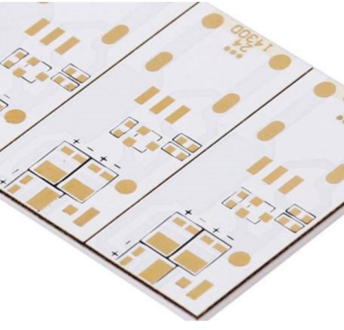
Direct bonded copper up to 0.4 mm for high-current power modules on alumina and AlN.

AMB

Active metal brazing on Si₃N₄ for EV inverters and thermal-cycling reliability.

DPC

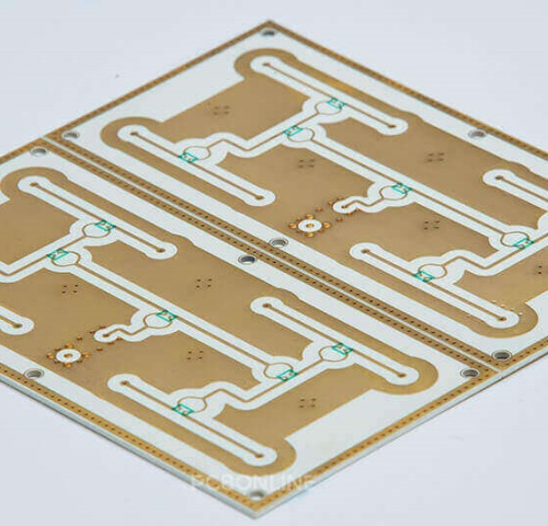
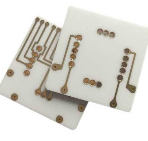
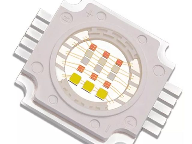
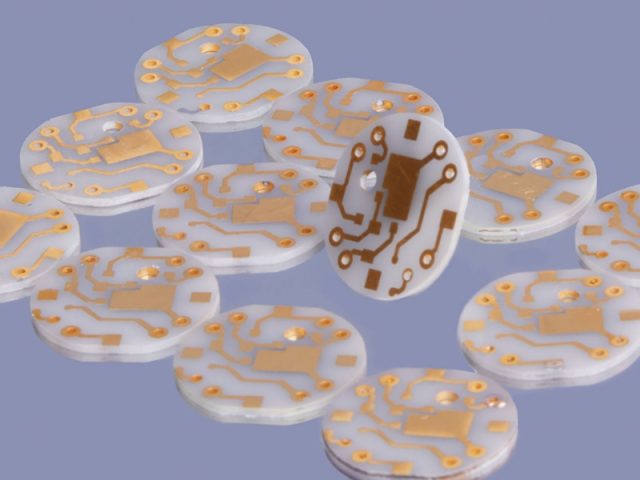
Direct plated copper with laser vias for fine-feature LED, sensor and RF substrates.

Thin Film

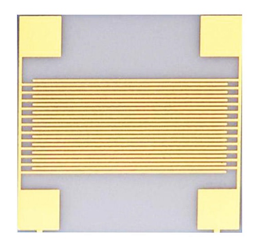
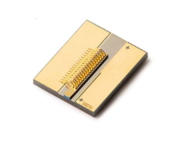
Sputtered Ti/Cu/Au down to ±10 µm lines for precision resistors and microwave circuits.

Thick Film

Screen-printed Ag/AgPd/Au conductors and resistors — cost-effective at volume.

HTCC / LTCC

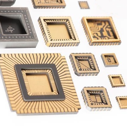
Co-fired multilayer ceramic for hermetic packages and RF/microwave modules.

ParameterAlumina / AlNDBC & AMBThin Film
Substrate thickness0.25 – 2.0 mm0.32 – 1.0 mm0.25 – 1.0 mm
Copper / metal thickness0.1 – 0.4 mm1 – 30 µm
Min line / space100 / 100 µm200 / 200 µm10 / 10 µm
Min laser via0.10 mm0.06 mm
Max panel size138 × 190 mm138 × 190 mm100 × 100 mm
Surface finishENIG · ENEPIG · Immersion Ag/Au · OSP · Sn
Layer count1 – 2Double-sidedMultilayer (LTCC 20+)
Application

Where ceramic earns its place.

Anywhere power density, temperature or frequency pushes FR-4 past its limits, ceramic takes over.

Products

A ceramic substrate for every stack-up.

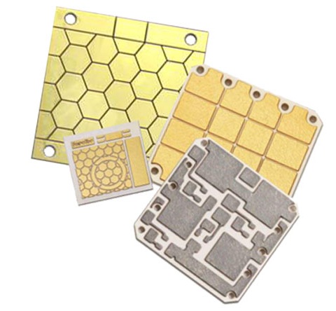
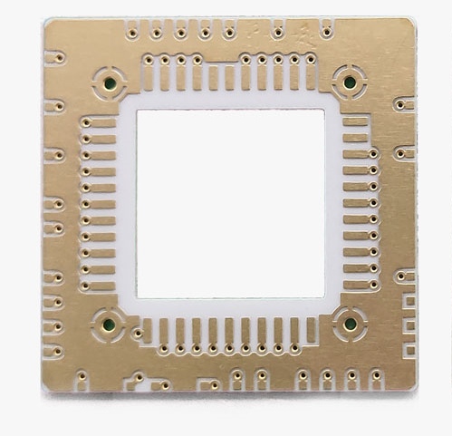
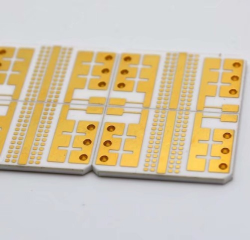
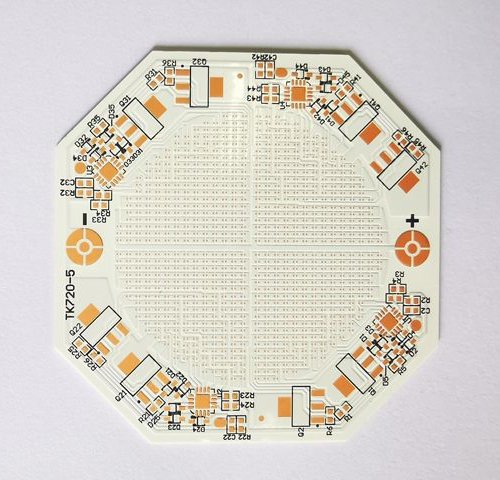
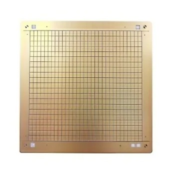
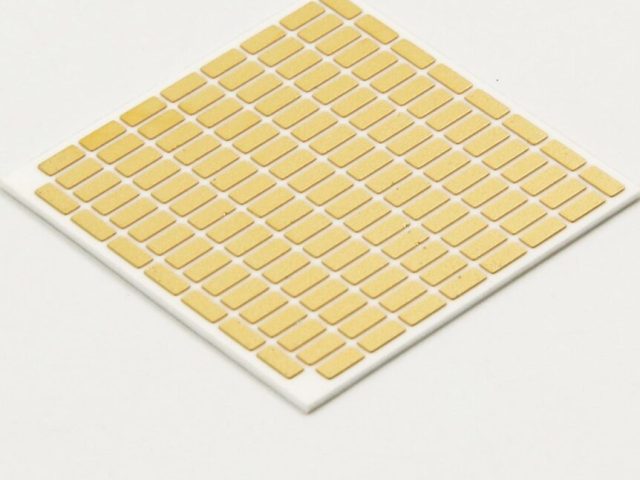
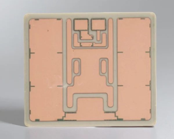
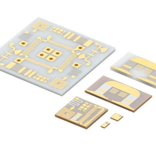
Representative parts across our processes. Every product is built to your drawing.

How we work

From your Gerber to qualified parts.

Share your design

Send Gerber, drawing or a sketch. Our engineers reply with DFM feedback in 24 h.

Material & process

We recommend the ceramic, metallization and finish for your thermal and cost target.

Prototype & qualify

Rapid prototypes in as little as 72 h, with dimensional and electrical reports.

Volume production

Qualified tooling scales with SPC, traceability and on-time delivery.

Contact Us

Send your drawing. Get a real quote.

Tell us the material, size and quantity — or just attach a file. A ceramic PCB engineer replies within one business day.

[email protected] +86 136 00427328
Thanks — your inquiry has been received. We reply within one business day.